PI74ALVCH162268A Ver la hoja de datos (PDF) - Pericom Semiconductor
Número de pieza
componentes Descripción
Lista de partido
PI74ALVCH162268A Datasheet PDF : 6 Pages
| |||
PI74ALVCH162268
1234567890123456789012345678901212345678901234567890112234-5B67i8t90T12o1223445-6B78i9t01R23e45g6i7s8t90e1r2e34d56B78u90s12E12x34c5h67a8n90g12e3r456w78i9t0h12334-5S67t8a90t1e21O23u45t6p78u9t01s2
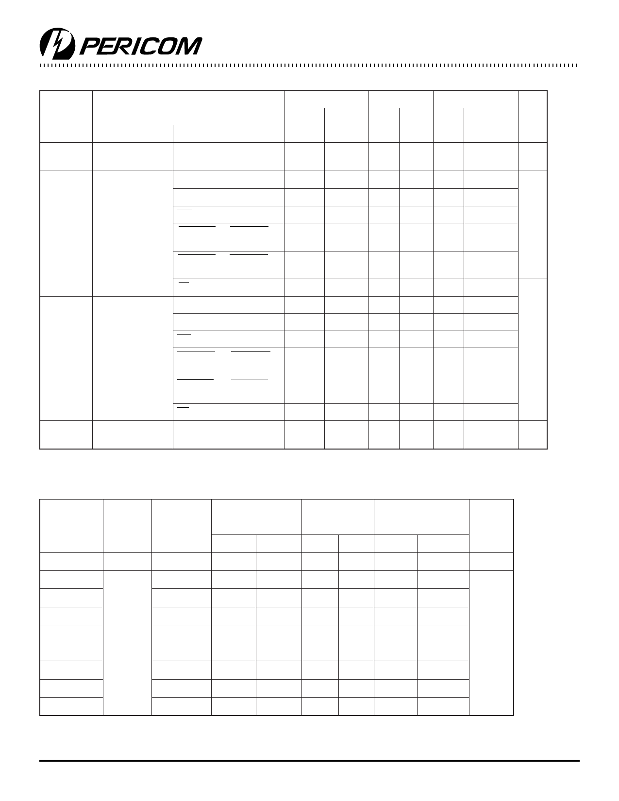
Timing Requirements over Operating Range
Parameters
Description
VCC= 2.5 V ± 0.2 V
Min.
Max.
VCC= 2.7 V
Min. Max.
fCLOCK
tW
Clock frequency
Pulse duration,
CLK high or Low
0
120
0
125
3.3
3.3
A data before CLK↑
4.5
4
B data before CLK↑
0.8
1.2
SEL before CLK↑
1.4
1.6
tSU
Setup time
CLKENA1 or CLKENA2
before CLK↑
3.6
3.4
CLKENB1 or CLKENB2
before CLK↑
3.2
3
OE before CLK↑
4.2
3.9
A data after CLK↑
0
0
B data after CLK↑
1.3
1.2
SEL after CLK↑
1
1
tH
Hold time
CLKENA1 or CLKENA2
after CLK↑
0.1
0.1
CLKENB1 or CLKENB2
after CLK↑
0.1
0
OE after CLK↑
0
0
∆t/∆v(1)
Input Transition
Rise or Fall
0
10
0
10
Notes:
1. Unused control inputs must be held HIGH or LOW to prevent them from floating.
VCC= 3.3 V ± 0.3 V
Min.
Max.
0
150
3.3
3.4
1
1.3
2.8
2.5
3.2
0.2
1.3
1
0.4
0.5
0.2
0
10
Units
Mhz
ns
ns
ns
ns/V
Switching Characteristics over Operating Range(1)
Parameters
From
(INPUT)
To
(OUTPUT)
VCC = 2.5V ± 0.2V
Min.(2)
Max.
VCC = 2.7V
Min.(2) Max.
VCC = 3.3V ± 0.3V
Min.(2)
Max.(2)
fMAX
120
125
150
tPD
B
1.6
6.1
5.9
1.8
5.4
tPD
A (1B)
1.6
5.8
5.4
1.7
4.8
tPD
B (2B)
1.6
5.8
5.3
1.8
4.8
tPD
A (SEL)
2.5
7.3
CLK
tEN
B
2.7
7.2
6.5
2.4
5.8
6.8
2.6
6.1
tDIS
B
2.8
7.2
6.1
2.5
5.9
tEN
A
2
6.2
5.6
1.8
5.1
tDIS
A
2
6.5
5.4
2.1
5
Notes:
1. Unused control inputs must be held HIGH or LOW to prevent them from floating.
2. Minimum limits are guaranteed but not tested on Propagation Delays.
Units
MHz
ns
5
PS8352 11/04/98
Share Link: 