SPT5110SCT Ver la hoja de datos (PDF) - Signal Processing Technologies
Número de pieza
componentes Descripción
Lista de partido
SPT5110SCT Datasheet PDF : 6 Pages
| |||
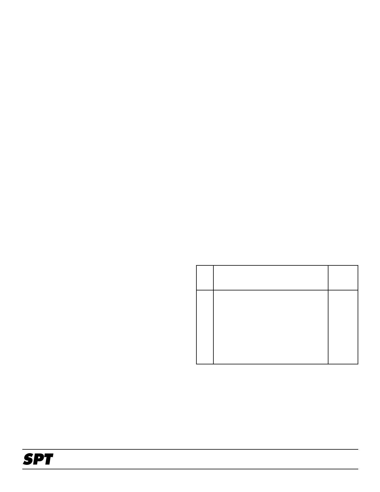
TEST LEVEL CODES
TEST LEVEL
All electrical characteristics are subject to the
I
following conditions: All parameters having min/
max specifications are guaranteed. The Test
II
Level column indicates the specific device test-
ing actually performed during production and
III
Quality Assurance inspection. Any blank sec-
IV
tion in the data column indicates that the speci-
fication is not tested at the specified condition.
V
VI
TEST PROCEDURE
100% production tested at the specified temperature.
100% production tested at TA=25 °C, and sample
tested at the specified temperatures.
QA sample tested only at the specified temperatures.
Parameter is guaranteed (but not tested) by design
and characterization data.
Parameter is a typical value for information purposes
only.
100% production tested at TA = 25 °C. Parameter is
guaranteed over specified temperature range.
INTERFACE CONSIDERATIONS
Figure 1 shows a typical interface circuit of the SPT5110 in
normal circuit operation.
SUPPLY AND GROUND CONSIDERATIONS
SPT suggests that all power supply pins (AVDD) be tied
together and decoupled using a 0.1 µF ceramic capacitor in
parallel with a 10 µF tantalum capacitor.
INTERNAL REFERENCE VOLTAGE (VREF)
Voltage reference is internally generated. Connect a 0.1 µF
bypass capacitor as close to the pin as possible.
FULL-SCALE ADJUST CONTROL (VCS)
Connect a 0.1 µF bypass capacitor with the shortest possible
lead length between VCS and AVSS. A resistor connected
between this pin and AVDD controls the magnitude of the full-
scale video signal.
The output voltage range of the SPT5110 can be kept
constant and stable by keeping the value of VCS to ground
constant. The full-scale voltage changes according to VCS.
(See figure 2.)
CURRENT OUTPUTS
Each red, green and blue current output should have a load
resistor connected to AVDD. The resistors are typically 240 Ω
and should be kept in the 150 Ω to 250 Ω range.
Table I - Binary Codes
1 LSB = 5.49 mV, VCS = 1.27 V
Step A7 A6
(MSB)
0 00
1 00
2 00
3 00
.
.
.
254 1 1
255 1 1
Digital Input
A5 A4 A3 A2
0000
0000
0000
0000
.
.
.
1111
1111
Analog
A1 A0 Out (V)
(LSB)
0 0 3.6000
0 1 3.6055
1 0 3.6110
1 1 3.6165
.
.
.
1 0 4.9890
1 1 4.9945
SPT
3
SPT5110
3/14/97
Share Link: 