PMB2304 Ver la hoja de datos (PDF) - Infineon Technologies
Número de pieza
componentes Descripción
Lista de partido
PMB2304 Datasheet PDF : 33 Pages
| |||
PMB 2304R
preliminary
Functional Description
8 NC
9 NC
10 FI
STDBY
11
VSS1
P in 1 0
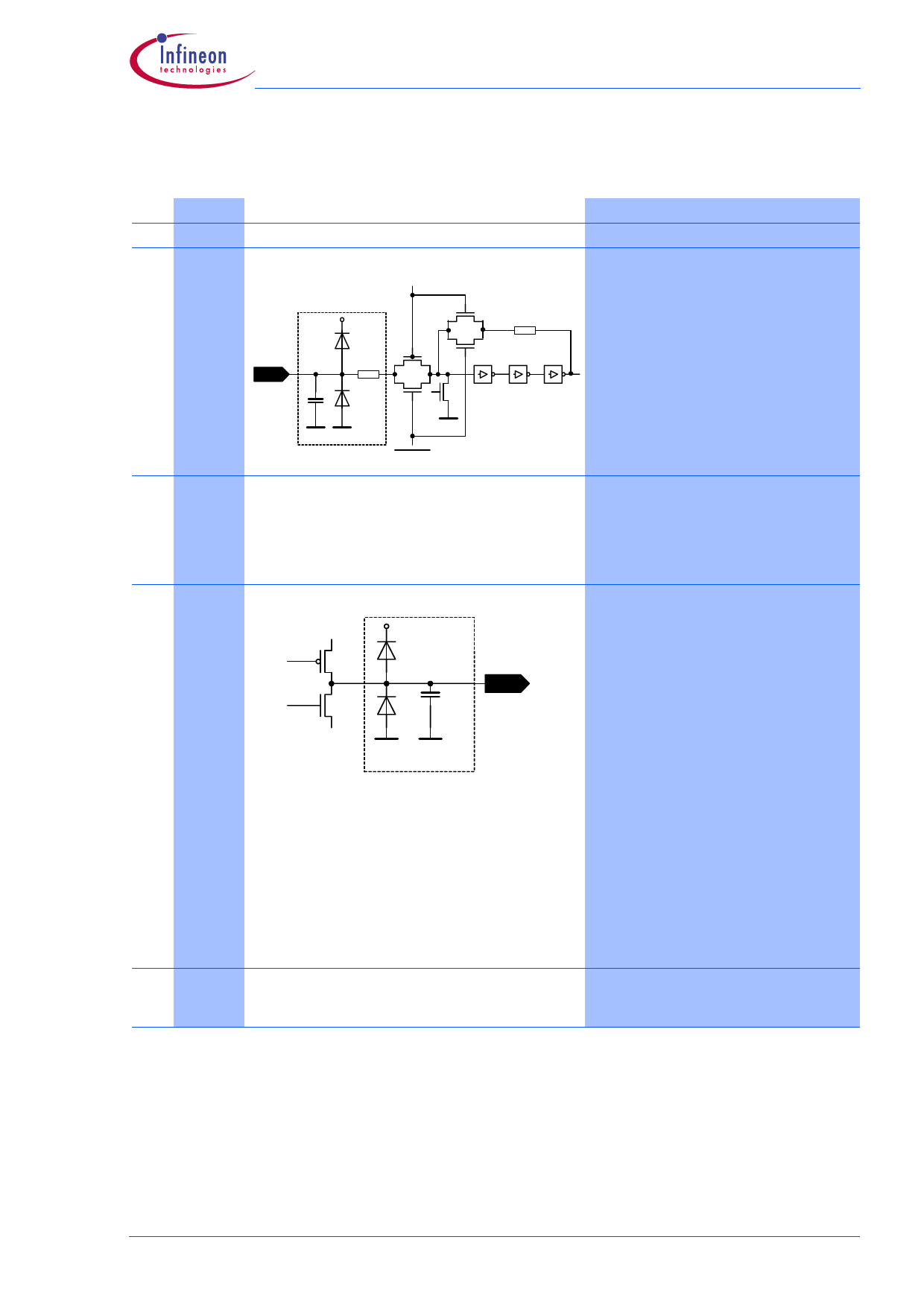
FI
560Ω
2pF
ESD
STDBY
500KΩ
12 PD
pin 12
*2pF
PD
ESD
* O nly this pin has lim ited build-in ESD
protection
13
VDD1
not connected
not connected
VCO-Frequency
Input with highly sensitive preamplifier for
14-bit N-counter and 7-bit A-counter. With
small input signals AC coupling must be
set up, where DC coupling can be used
for large input signals.
Ground for the preamplifiers, counters,
phase detector and charge pump.
(Note: The pins VDD and VDD1 respec-
tively VSS and VSS1 have to have the
same supply voltage.)
Phase Detector
Tristate charge pump output. The inte-
grated, positive and negative current
sources can be programmed with respect
to their current density by means of the
serial control. Activation and deactivation
depend on the phase relationship of the
scaled-down input signals FI:N, RI:R.
(See phase detector output waveforms.)
frequencyfV < fR or fV lagging:p-channel
current source active
frequencyfV > fR or fR leading:n-channel
current source active
frequencyfV = fR and PLL locked:current
sources are switched off,
PD-output is tristate
In standby mode the PD-output is set to
tristate. The assignment of the current
sources to the output signals of the phase
detector can be swapped in it’s polarity,
i.e. the sign of the phase detector con-
stant can be controlled.
Positive supply voltage for the preamplifi-
ers, counters, phase detector and charge
pump.
Wireless Components
3-4
Specification, June 2002
Share Link: 