R3113D441X Ver la hoja de datos (PDF) - RICOH Co.,Ltd.
Número de pieza
componentes Descripción
Lista de partido
R3113D441X Datasheet PDF : 18 Pages
| |||
R3113D
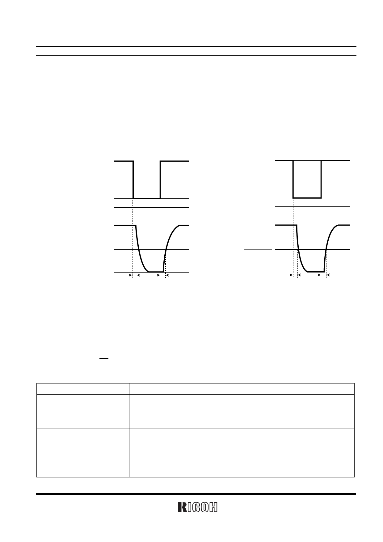
DEFINITION OF OUTPUT DELAY TIME
Output Delay Time tPLH is defined as follows:
1. In the case of Nch Open Drain Output:
Under the condition of the output pin (OUT) is pulled up through a resistor of 470kΩ to 5V, the time interval
between the rising edge of VDD pulse from 0.85V to (+VDET)+ 1.0V and becoming of the output voltage to 2.5V.
2. In the case of CMOS Output:
The time interval between the rising edge of VDD pulse from 0.85V to (+VDET)+ 1.0V and becoming of the
output voltage to (VDD/2) V.
+VDET + 1.0V
Input Voltage
(VDD)
0.85V
GND
+VDET + 1.0V
Input Voltage
(VDD)
0.85V
GND
Output Voltage
5.0V
2.5V
+VDET+1.0V
Output Voltage
+VDET+1.0V
2
GND
tPHL
tPLH
Nch Open Drain Output
GND
tPHL
tPLH
CMOS Output
SELECTION GUIDE
The detector threshold, the output type and the taping type of R3113 Series can be designated at the users’
request by specifying the part number as follows;
R3113xxx1x-xx ← Part Number
↑↑ ↑ ↑
ab c d
Code
a
b
c
d
Contents
Designation of Package Type;
SON1408-3
Setting Detector Threshold (−VDET);
Stepwise setting with a step of 0.1V in the range of 1.2V to 4.5V is possible.
Designation of Output Type;
A: Nch Open Drain
C: CMOS
Designation of Packing or Taping Type;
Ex.TR prescribed as standard directions.
(Refer to Taping Specifications.) Antistatic bag for samples: C
3
Share Link: 