R3113D Ver la hoja de datos (PDF) - RICOH Co.,Ltd.
Número de pieza
componentes Descripción
Lista de partido
R3113D Datasheet PDF : 18 Pages
| |||
R3113D
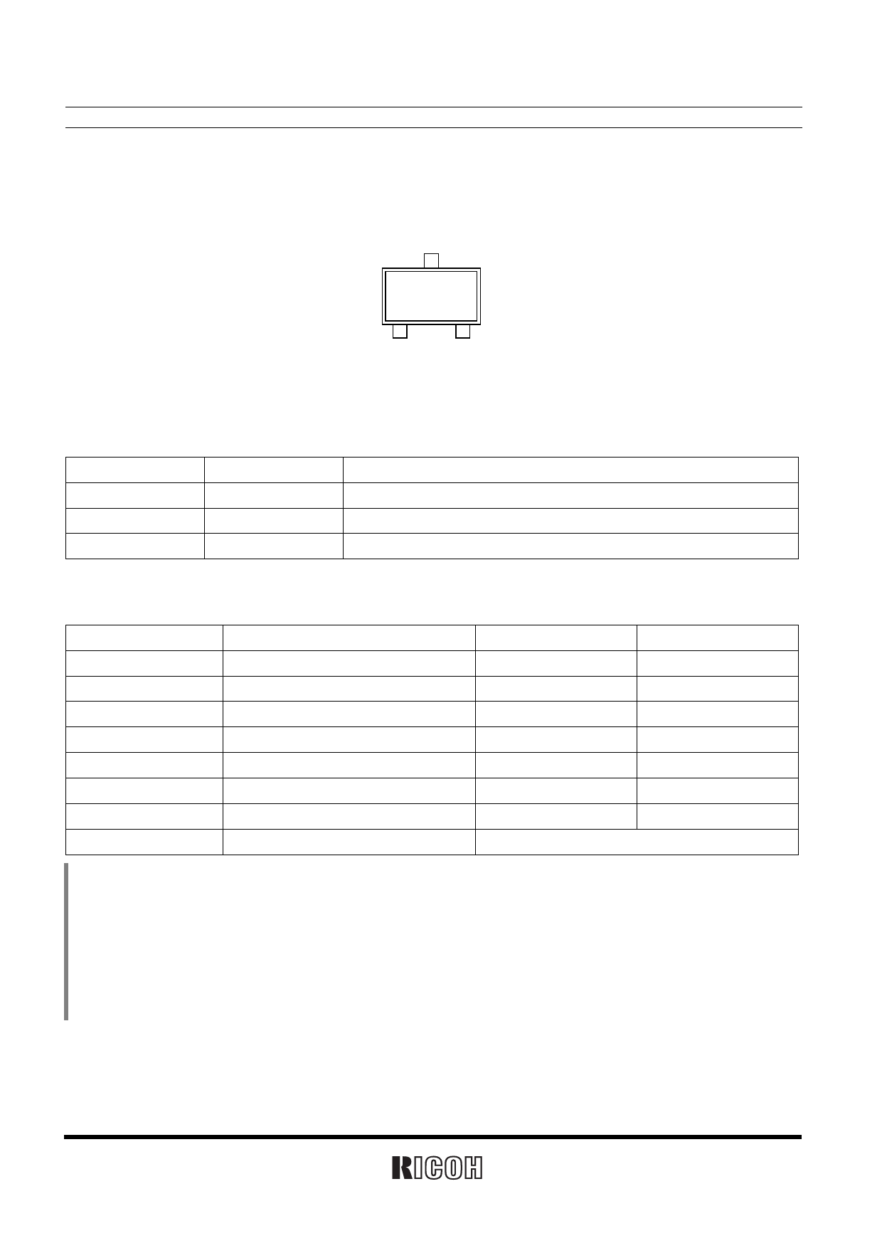
PIN CONFIGURATION
SON1408-3
3
(mark side)
1
2
PIN DESCRIPTION
• R3113D
Pin No.
1
2
3
Symbol
OUT
VDD
GND
Output Pin
Input Pin
Ground Pin
Description
ABSOLUTE MAXIMUM RATINGS
Symbol
VDD
VOUT1
VOUT2
IOUT
PD
Topt
Tstg
Tsolder
Item
Supply Voltage
Output Voltage (CMOS)
Output Voltage (Nch)
Output Current
Power Dissipation∗Note1
Operating Temperature Range
Storage Temperature Range
Lead temperature (Soldering)
Rating
6.5
VSS−0.3 to VDD+0.3
VSS−0.3 to 6.5
20
250
−40 to 85
−55 to 125
260°C, 10s
Unit
V
V
V
mA
mW
°C
°C
∗Note 1: Applied to SON1408-3 at mounted on board
PD depends on conditions of mounting on board.
This specification is based on the measurement at the condition below:
∗Measurement Conditions
Environment: Mounted on board (Wind velocity 0m/s)
Board Material: FR-4 (2-layer)
Board dimensions: 40mm × 40mm × t1.6mm
Copper Area: 50%(Both Sides)
Tab pin (Pin 3) land pattern width is same as the lead, connected to the GND plane.
4
Share Link: 