RF2362PCBA-41X Ver la hoja de datos (PDF) - RF Micro Devices
Número de pieza
componentes Descripción
Lista de partido
RF2362PCBA-41X Datasheet PDF : 10 Pages
| |||
RF2362
Pin Function Description
Interface Schematic
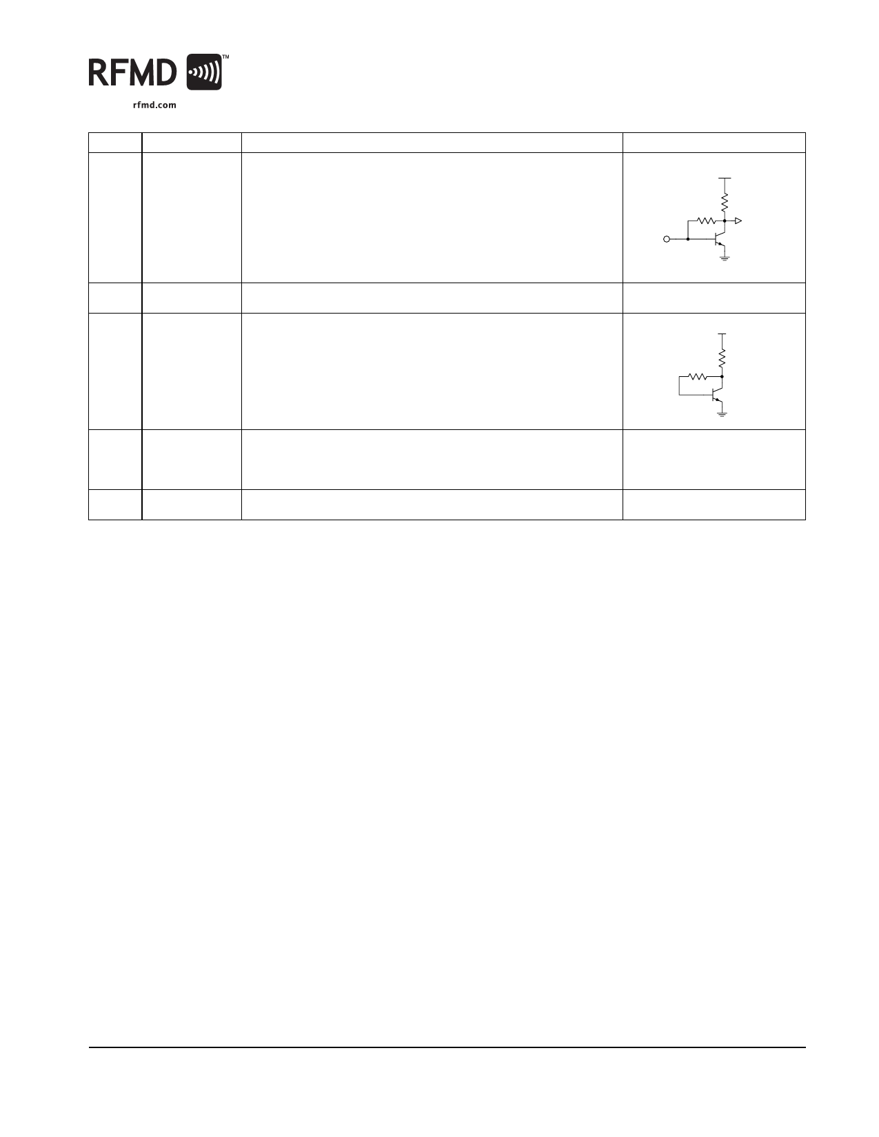
1
RF IN
RF input pin. This pin is DC-coupled and matched to 50Ω at 1880MHz.
PD
RF IN
2
GND1
Ground connection. For best performance, keep traces physically short
and connect immediately to ground plane.
3
VPD
Power Down for the IC. VPD = 2.8V +/- 0.1V turns on the part. VPD<0.9V
turns off the part. External RF bypassing is required. The trace length
between the pin and the bypass capacitors should be minimized. The
ground side of the bypass capacitors should connect immediately to
ground plane. Nominal current required for VPD = 2.8V is 8.5 mA typical
and 12 mA Max (@VPD =2.9 V).
4
RF OUT
Amplifier Output pin. This pin is an open-collector output. It must be biased
to either VCC or pin 4 through a choke or matching inductor. This pin is typi-
cally matched to 50Ω with a shunt bias/matching inductor and series
blocking/matching capacitor. Refer to application schematics.
5
GND2
Ground connection. For best performance, keep traces physically short
and connect immediately to ground plane.
TO OUTPUT
STAGE
PD
Rev A6 DS070816
7628 Thorndike Road, Greensboro, NC 27409-9421 · For sales or technical
support, contact RFMD at (+1) 336-678-5570 or sales-support@rfmd.com.
3 of 10
Share Link: 