RF2367PCBA-41X Ver la hoja de datos (PDF) - RF Micro Devices
Número de pieza
componentes Descripción
Lista de partido
RF2367PCBA-41X Datasheet PDF : 10 Pages
| |||
RF2367
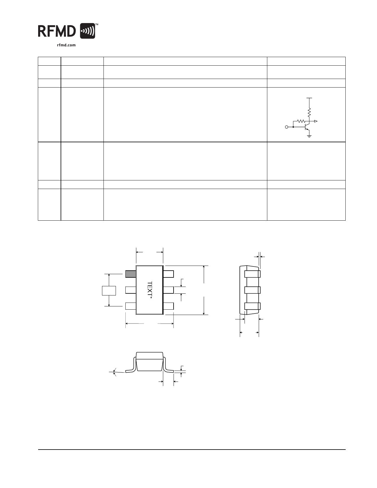
Pin Function Description
Interface Schematic
1
GND
Ground connection. Keep traces physically short and connect immediately
to ground plane for best performance.
2
GND
Same as pin 1.
3
RF IN
RF input pin. This pin is DC coupled and internally matched to a <2:1 VSWR
at 1880MHz.
PD
RF IN
4
PD
Power Down for the IC. VPD = 2.8V +/- 0.1V turns on the Part. VPD<0.9V See pin 3.
turns off the Part. Lower threshold for device operation is approximately
1.2V. External RF bypassing is required. The trace length between the pin
and the bypass capacitors should be minimized. The ground side of the
bypass capacitors should connect immediately to ground plane. Nominal
current for this pin for VPD = 2.8V is 8mA typical.
5
GND
Same as pin 1.
6
RF OUT
Amplifier Output pin. This pin is an open-collector output. It must be biased
to either VCC or pin 4 through a choke or matching inductor. This pin is typi-
cally externally matched to 50Ω with a shunt bias/matching inductor and
series blocking/matching capacitor. Refer to application/evaluation board
schematics.
Package Drawing
1.80
1.40
0.10
MAX.
1.90
0.50
0.35 3.10
2.70
3.00
2.60
Shaded lead is pin 1.
Dimensions in mm.
0.90
0.70
1.30
1.00
9°
0.25 *When Pin 1 is in upper left,
1°
0.10 text reads downward
(as shown).
0.37 MIN.
TO OUTPUT
STAGE
Rev A3 DS060925
7628 Thorndike Road, Greensboro, NC 27409-9421 · For sales or technical
support, contact RFMD at (+1) 336-678-5570 or sales-support@rfmd.com.
3 of 10
Share Link: 