RF2637 Ver la hoja de datos (PDF) - RF Micro Devices
Número de pieza
componentes Descripción
Lista de partido
RF2637 Datasheet PDF : 10 Pages
| |||
RF2637
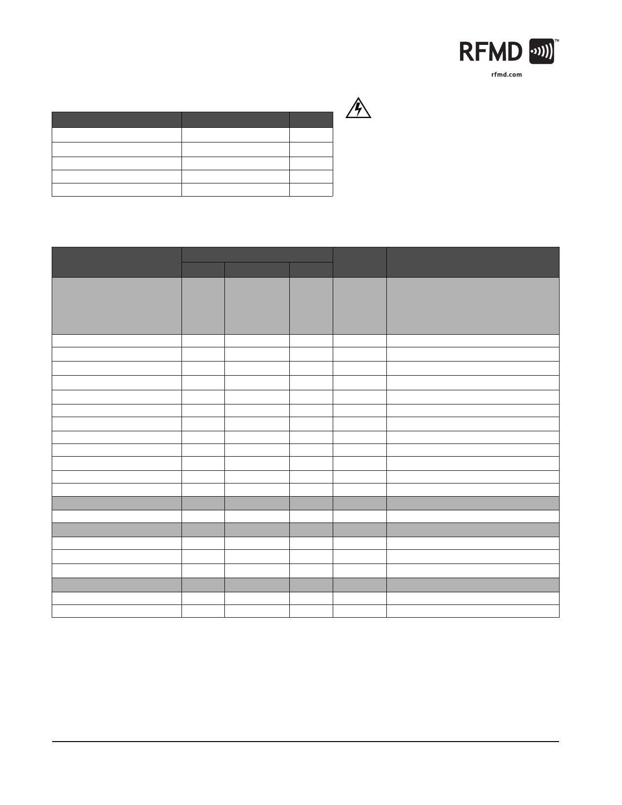
Absolute Maximum Ratings
Parameter
Supply Voltage
Control Voltage
Input RF Power
Operating Ambient Temperature
Storage Temperature
Value
-0.5 to +5.0
-0.5 to +5.0
+10
-40 to +85
-40 to +150
Unit
VDC
VDC
dBm
°C
°C
Caution! ESD sensitive device.
Exceeding any one or a combination of the Absolute Maximum Rating conditions may
cause permanent damage to the device. Extended application of Absolute Maximum
Rating conditions to the device may reduce device reliability. Specified typical perfor-
mance or functional operation of the device under Absolute Maximum Rating condi-
tions is not implied.
RoHS status based on EUDirective2002/95/EC (at time of this document revision).
The information in this publication is believed to be accurate and reliable. However, no
responsibility is assumed by RF Micro Devices, Inc. ("RFMD") for its use, nor for any
infringement of patents, or other rights of third parties, resulting from its use. No
license is granted by implication or otherwise under any patent or patent rights of
RFMD. RFMD reserves the right to change component circuitry, recommended appli-
cation circuitry and specifications at any time without prior notice.
Parameter
Specification
Min.
Typ.
Max.
Overall
Frequency Range
12 to 385
Maximum Gain
+40
+51
+65
Minimum Gain
-65
-55
-40
Maximum Gain
+35
+45
+55
Minimum Gain
-68
-58
-48
Gain Slope
57
Gain Control Voltage Range
0 to 2.5
Gain Control Input Impedance
30
Noise Figure
5
7.2
Input IP3
-46
-40
-2
Stability (Max VSWR)
10:1
IF Input
Input Impedance
1
Power Supply
Voltage
2.7 to 3.4
Current Consumption
6
10
15
7
11.5
15
Thermal
Thermal Resistance
150
Maximum Junction Temperature
90
Note 1: Measured between a gain control voltage of 1.0V to 1.5V.
Unit
MHz
dB
dB
dB
dB
dB/V
VDC
kΩ
dB
dBm
dBm
Condition
T=25°C, 85MHz, VCC=3.0V, ZS =500Ω,
ZL=500Ω, 500Ω External Input Terminating
Resistor, 500Ω External Output Terminating
Resistor (Effective ZS=333Ω, Effective
ZL=250Ω) (See Application Example)
VGC=2.5V, 85MHz
VGC=0.1V, 85MHz
VGC=2.5V, 385MHz
VGC=0.1V, 385MHz
Note 1
Source impedance of 4.7kΩ
At maximum gain and 85MHz
At +40dB gain, referenced to 500Ω
At minimum gain, referenced to 500Ω
Spurious < -70 dBm
kΩ
CDMA, differential
V
mA
Minimum gain, VCC=3.0V
mA
Maximum gain, VCC=3.0V
°C/W
°C
Theta J-Ref 85°C
Ref 85°C
2 of 10
7628 Thorndike Road, Greensboro, NC 27409-9421 · For sales or technical
support, contact RFMD at (+1) 336-678-5570 or sales-support@rfmd.com.
Rev A5 DS050829
Share Link: 