RF2637 Ver la hoja de datos (PDF) - RF Micro Devices
Número de pieza
componentes Descripción
Lista de partido
RF2637 Datasheet PDF : 10 Pages
| |||
RF2637
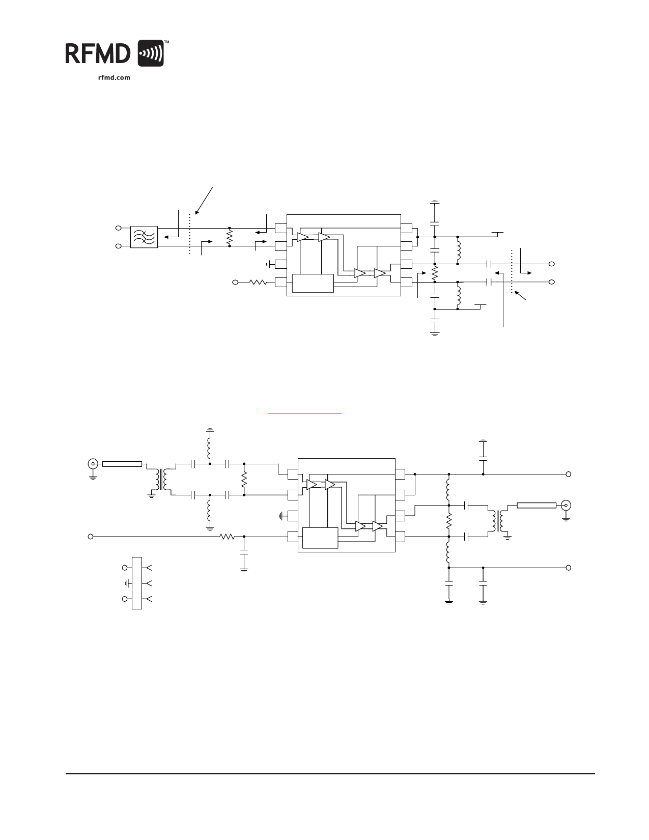
Application Schematic
C
D
M
A
I
F
F
i
l
t
e
r
CDMA+
CDMA-
M easurem ent
R eference P lane
ZS=500 Ω
Z S, EFF=333 Ω
Z IN, EFF= 5 0 0 Ω
1
R1:
1 kΩ
2
Z IN= 1 k Ω
3
G AIN
4
G A IN
4.7 kΩ
CONTROL
8
7
6
5
Z LO AD,EFF= 2 5 0 Ω
R 1 sets the C D M A balanced input im pedance. T he effective input im pedance is then 500 Ω .
R 2 sets the balanced output im pedance to 500 Ω . L1 and C 2 serve dual purposes. L1 serves
as an output bias choke , and C 2 serves as a series D C block. In addition, the values of L1 and
C 2 m ay be chosen to form an im pedance m atching netw ork of the load im pedance is not 500
Ω . O therw ise, the values of L1 and C 1 are chosen to form a parallel-resonant tank circuit at
the IF w hen the load im pedance is 500 Ω .
10 nF
V CC
C1 L1
C2
R2: 500Ω C2
ZLOAD=500Ω
OUT+
OUT-
C1 L1
V CC
M easurem ent
R eference P lane
10 nF
ZOUT=500 Ω
Evaluation Board Schematic
(Download Bill of Materials from www.rfmd.com.)
CDMA
J1
SMA
50 Ω μstrip
T1
GC
P1
P1-1 1 VCC
2 GND
P1-3 3 GC
C3
L1
15 pF 390 nH
C4
15 pF
C1
R1
10 nF 1 kΩ
L2
C2
390 nH 10 nF
R2
4.7 kΩ
C5
1 nF
1
2
3
4
GAIN
CONTROL
2627400A
C10
10 nF
8
VCC
L4
C8
7
390nH 15 pF
OUT
J2
6
R3
T2
50 Ω μstrip
SMA
510 Ω
5
L3
390nH
C9
15 pF
VCC
C6
10 nF
C7
10 nF
Rev A5 DS050829
7628 Thorndike Road, Greensboro, NC 27409-9421 · For sales or technical
support, contact RFMD at (+1) 336-678-5570 or sales-support@rfmd.com.
5 of 10
Share Link: 