RF2705GPCBA-41X Ver la hoja de datos (PDF) - RF Micro Devices
Número de pieza
componentes Descripción
Lista de partido
RF2705GPCBA-41X Datasheet PDF : 26 Pages
| |||
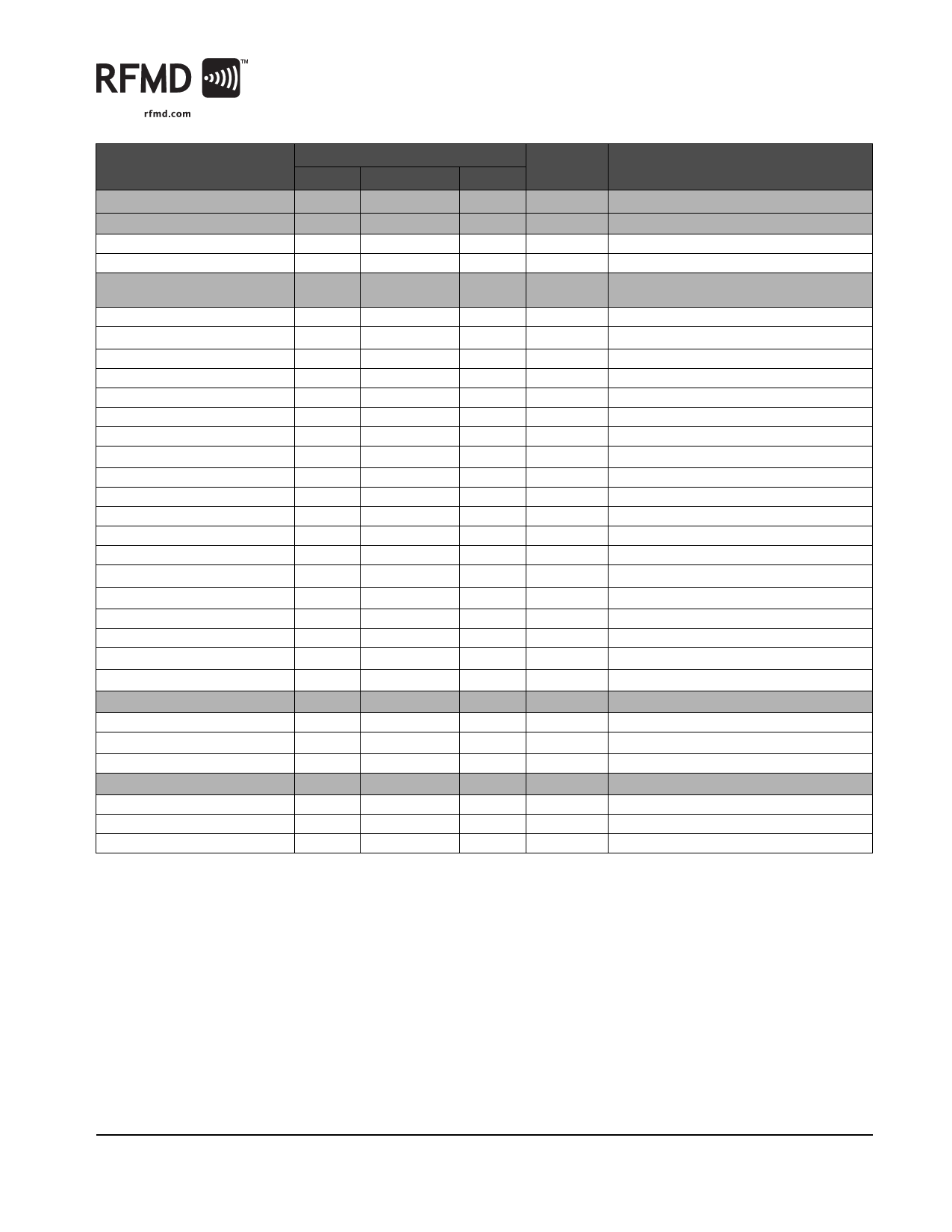
RF2705G
Parameter
General Specifications
Operating Range
Supply Voltage
Temperature
Current Consumption
Sleep
Wideband FLOx1 (high power)
*
(medium power)
*
(low power)
*
Wideband FLOx2 (high power)
(medium power)
(low power)
High Band FLOx2
Low Band FLO/2
High Band Bypass
Low Band Bypass
Logic Levels
High Band FLOx1
Low Band FLOx1
Input Logic 0
Input Logic 1
Logic Pins Input Current
LO Input Ports
LO LB Input Frequency Range
LO HB Input Frequency Range
Input Impedance
Min.
2.7
-40
0
1.4
800
1600
Specification
Typ.
Max.
<1
114
85
89
54
63
42
110
84
80
53
54
41
72
82
23
22
76
74
<1.0
50
3.3
+85
10
0.4
VCC
1000
2000
Unit
Condition
V
°C
Refer to Logic Control Truth Table for Mode
Control Pin Voltages.
μA
mA
GC = 2.0 V
mA
GC = 0.2 V
mA
GC = 2.0 V
mA
GC = 0.2 V
mA
GC=2.0V. See Note 1.
mA
GC=0.2V. See Note 1.
mA
GC = 2.0 V
mA
GC = 0.2 V
mA
GC = 2.0 V
mA
GC = 0.2 V
mA
GC=2.0V. See Note 1.
mA
GC=0.2V. See Note 1.
mA
GC = 2.0 V
mA
GC = 2.0 V
mA
mA
mA
GC = 2.0 V
mA
GC = 2.0 V
V
V
μA
CMOS inputs
MHz
MHz
Ω
Externally matched
Rev A0 DS060206
7628 Thorndike Road, Greensboro, NC 27409-9421 · For sales or technical
support, contact RFMD at (+1) 336-678-5570 or sales-support@rfmd.com.
11 of 26
Share Link: 