RF3854 Ver la hoja de datos (PDF) - RF Micro Devices
Número de pieza
componentes Descripción
Lista de partido
RF3854 Datasheet PDF : 26 Pages
| |||
RF3854
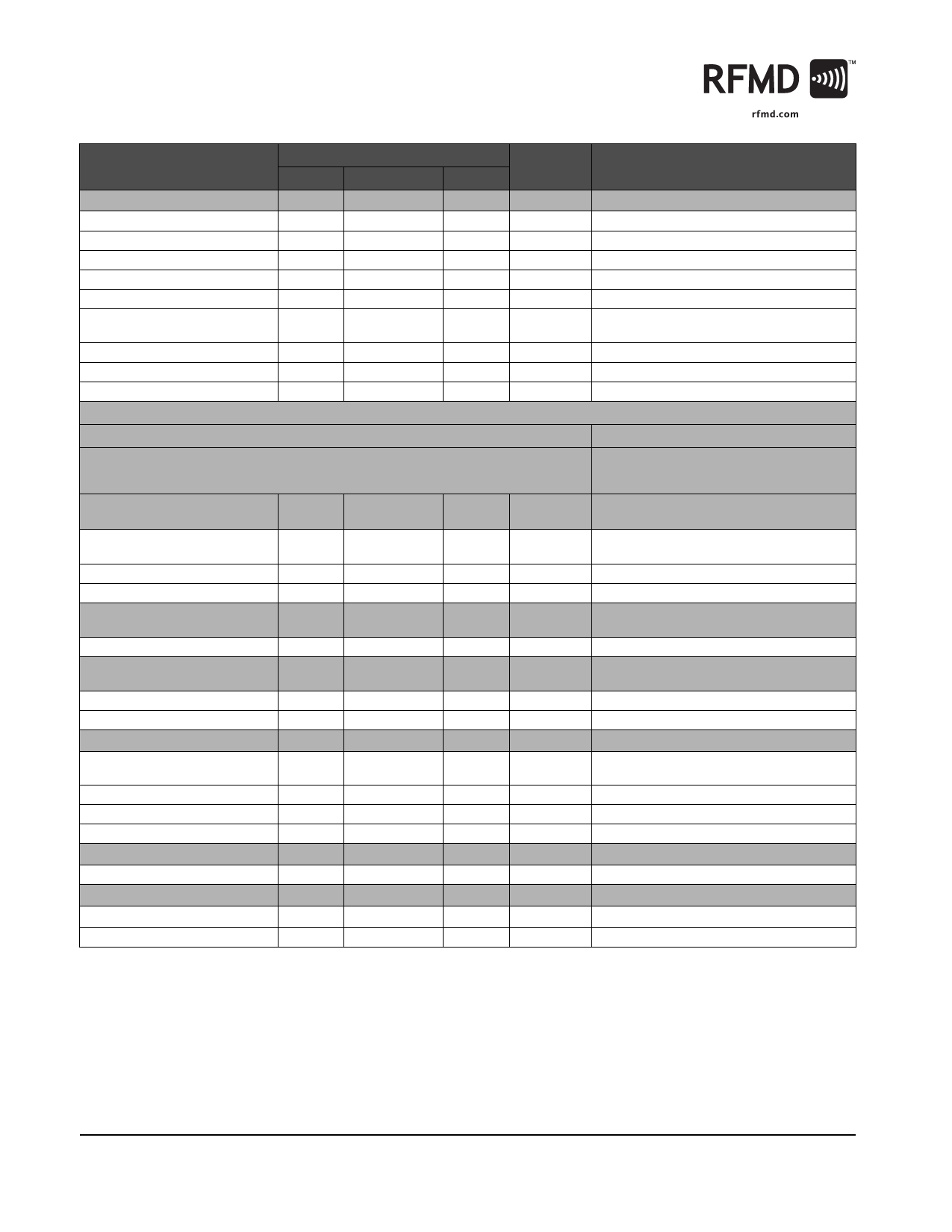
Parameter
General Conditions
Local Oscillator
LO HB Input Frequency
RF HB Output Frequency
Input Power
IQ Baseband Inputs
IQ Level
Min.
1710
1710
-6.0
Specification
Typ.
Max.
1910
1910
0.0
+3.0
1.2
Unit
MHz
MHz
dBm
VP-P
IQ Common Mode
1.2
V
Input Bandwidth 0.7
1.0
MHz
Baseband Filter Attenuation 20
dB
Output Performance with Modulated Baseband Inputs
W-CDMA Mode
Mode=Wideband FLOx2 (see Control Logic Truth Table for Mode Control
Settings)
Output Power
Maximum Output Power with
W-CDMA Modulated Signal*
High Power Mode
3
Medium Power Mode
-4
Gain Range
High Power Mode
Gain Step
High Power to Medium Power
Medium Power to Low Power
Out-of-Band Emission
Adjacent Channel Leakage Power
Ratio (ALCR)*
Channel Spacing
±5 MHz
±10 MHz
Error Vector Magnitude
RMS*
Output Noise
At FC±40MHz*
* Not tested in Production
6
dBm
-1
dBm
90
dB
±0.5
dB
TBD
dB
50
65
1.4
-152
-146
-146
dBc
dBc
%rms
dBc/Hz
dBc/Hz
Condition
8PSK
Input IQ signal driven differentially and in
quadrature.
At 20MHz offset
VCC=2.7V, T=+25°C, while meeting 48dBc
ALCR
GC = 2.0 V
GC = 1.5 V
Difference between output power at GC=2.0V
and GC=0.2V.
Gain step when switching between power
modes in either direction.
GC = 1.4 V
GC = TBD
3.84MHz relative to channel power
3.84MHz relative to channel power
3GPP W-CDMA
GC = 2.0 V
GC=2.0V to 1.5V
4 of 26
7628 Thorndike Road, Greensboro, NC 27409-9421 · For sales or technical
support, contact RFMD at (+1) 336-678-5570 or sales-support@rfmd.com.
Rev A1 DS070313
Share Link: 