CY7C185-20PC(1996) Ver la hoja de datos (PDF) - Cypress Semiconductor
Número de pieza
componentes Descripción
Lista de partido
CY7C185-20PC Datasheet PDF : 10 Pages
| |||
FOR REVIEW ONLY
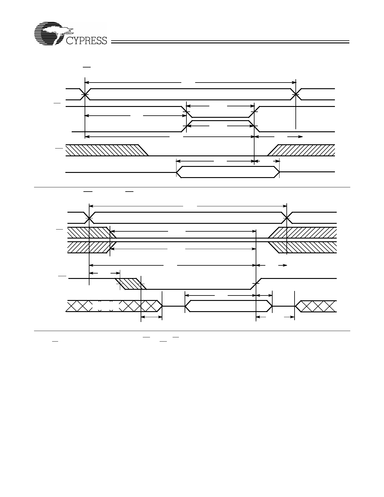
Switching Waveforms (continued)
Write Cycle no.2 (CE Controlled)[12,13,15]
ADDRESS
CE1
tSA
CE2
WE
DATA I/O
tWC
tSCE1
tSCE2
tAW
tHA
tSD
tHD
DATA IN VALID
CY7C185
C185–9
Write Cycle No.3 (WE Controlled, OE LOW)[12,13,14,15]
tWC
ADDRESS
CE1
tSCE1
CE2
tSCE2
tAW
tSA
WE
DATA I/O
NOTE 15
tHZWE
tSD
DATA IN VALID
tHA
tHD
tLZWE
C185–10
Notes:
9. Device is continuously selected. OE, CE1 = VIL. CE2 = VIH.
10. WE is HIGH for read cycle.
11. Data I/O is High Z if OE = VIH, CE1 = VIH, WE = VIL or CE2=VIL.
12. The internal write time of the memory is defined by the overlap of CE1 LOW, CE2 HIGH and WE LOW. CE1 and WE must be LOW and CE2 must be HIGH
to initiate write. A write can be terminated by CE1 or WE going HIGH or CE2 going LOW. The data input set-up and hold timing should be referenced to the
rising edge of the signal that terminates the write.
13. The minimum write cycle time for write cycle #3 (WE controlled, OE LOW) is the sum of tHZWE and tSD.
14. If CE1 goes HIGH or CE2 goes LOW simultaneously with WE HIGH, the output remains in a high-impedance state.
15. During this period, the I/Os are in the output state and input signals should not be applied.
6
Share Link: 