RT8279 Ver la hoja de datos (PDF) - Richtek Technology
Número de pieza
componentes Descripción
Lista de partido
RT8279 Datasheet PDF : 14 Pages
| |||
RT8279
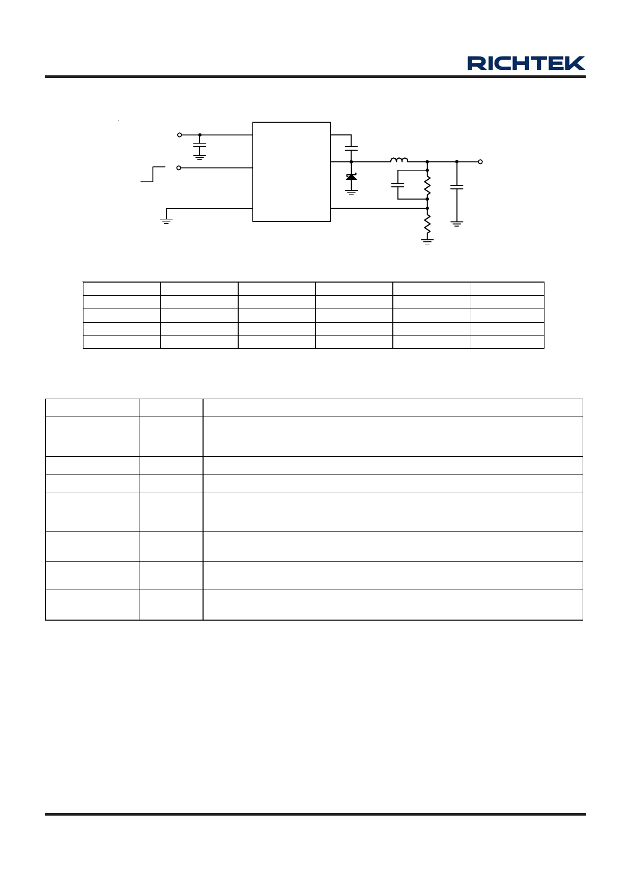
Typical Application Circuit
VIN
5.5V to 36V
Chip Enable
CIN
4.7µF/
50V x 2
Open = Automatic
Startup
7 VIN
BOOT 1
RT8279
5 EN
SW 8
6, 9 (Exposed Pad)
GND
FB 4
CBOOT
10nF L1
D1
B550A
CFF R1
R2
VOUT
COUT
22µF x 2
VOUT (V)
2.5
3.3
5
8
Table 1. Recommended Component Selection
R1 (kΩ)
100
R2 (kΩ)
100
CFF (pF)
82
L (μH)
6.8
100
58.6
82
10
100
31.6
82
15
100
18
82
22
COUT (μF)
22 x 2
22 x 2
22 x 2
22 x 2
Functional Pin Description
Pin No.
Pin Name
Pin Function
High Side Gate Drive Boost Input. BOOT supplies the drive for the high side
1
BOOT
N-MOSFET switch. Connect a 10nF or greater capacitor from SW to BOOT to
power the high side switch.
2, 3
NC
No Internal Connection.
4
FB
Feedback Input. The feedback threshold is 1.222V.
Enable Input. EN is a digital input that turns the regulator on or off. Drive EN
5
EN
higher than 1.4V to turn on the regulator, lower than 0.4V to turn it off. For
automatic startup, leave EN unconnected.
6,
9 (Exposed Pad)
GND
Ground. The exposed pad must be soldered to a large PCB and connected to
GND for maximum power dissipation.
7
VIN
Power Input. A suitable large capacitor should be bypassed from VIN to GND to
eliminate noise on the input to the IC.
8
SW
Power Switching Output. Note that a capacitor is required from SW to BOOT to
power the high side switch.
www.richtek.com
2
DS8279-01 December 2011
Share Link: 