RT9017 Ver la hoja de datos (PDF) - Richtek Technology
Número de pieza
componentes Descripción
Lista de partido
RT9017 Datasheet PDF : 12 Pages
| |||
Preliminary
RT9017
For continuous operation, do not exceed absolute
maximum operation junction temperature 125°C. The
power dissipation definition in device is :
PD = (VIN − VOUT) x IOUT + VIN x IQ
The maximum power dissipation depends on the thermal
resistance of IC package, PCB layout, the rate of
surroundings airflow and temperature difference between
junction to ambient. The maximum power dissipation can
be calculated by following formula :
PD(MAX) = ( TJ(MAX) - TA ) / θJA
Where TJ(MAX) is the maximum operation junction
temperature 125°C, TA is the ambient temperature and the
θJA is the junction to ambient thermal resistance.
For recommended operating conditions specification of
RT9017, where TJ(MAX) is the maximum junction
temperature of the die (125°C) and TA is the maximum
ambient temperature. The junction to ambient thermal
resistance (θJA is layout dependent) for SOT-23-3/SOT-
23-5 package is 250°C/W and WDFN-6L 2x2 package is
165°C/W on standard JEDEC 51-3 thermal test board.
The maximum power dissipation at TA = 25°C can be
calculated by following formula :
PD(MAX) = (125°C−25°C)/250 = 400 mW (SOT-23-3/
SOT-23-5)
PD(MAX) = (125°C−25°C)/333 = 300 mW (SC-70-5)
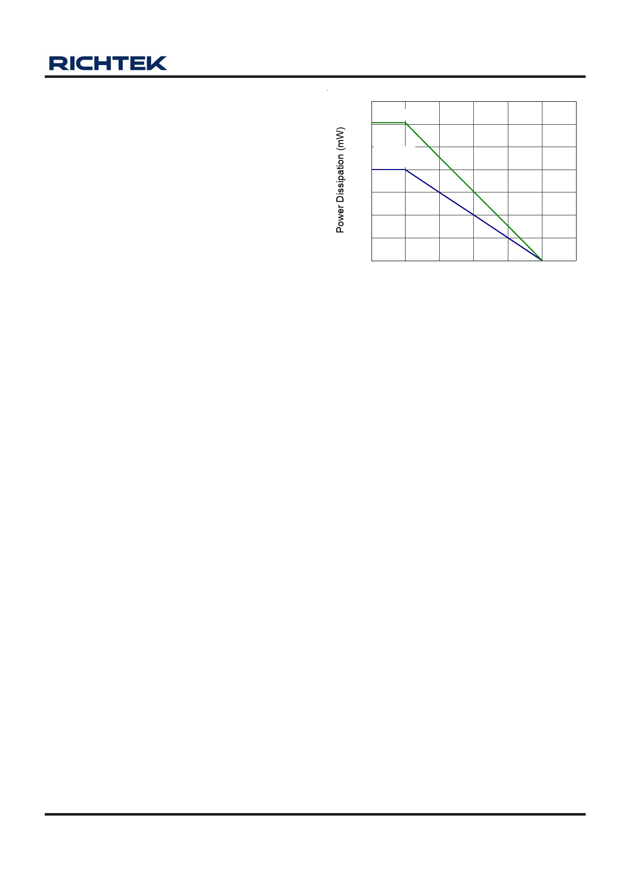
The maximum power dissipation depends on operating
ambient temperature for fixed TJ(MAX) and thermal
resistance θJA. For RT9017 packages, the Figure 3. of
derating curves allows the designer to see the effect of
rising ambient temperature on the maximum power
allowed.
700
WDFN-6L 2x2
600
500 SOT-23-3/
SOT-23-5
400
300
200
100
0
0
25
50
75
100 125 150
Ambient Temperature (°C)
Figure 3. Derating Curve for Packages
DS9017-03 August 2007
www.richtek.com
9
Share Link: 