RT9173 Ver la hoja de datos (PDF) - Richtek Technology
Número de pieza
componentes Descripción
Lista de partido
RT9173 Datasheet PDF : 13 Pages
| |||
RT9173/A
Application Information
Internal Parasitic Diode
Avoid forward-bias internal parasitic diode, VOUT to VCNTL,
and VOUT to VIN, the VOUT should not be forced some
voltage respect to ground on this pin while the VCNTL or
VIN is disappeared.
Consideration while Designs the Resistance of
Voltage Divider
Make sure the sinking current capability of pull-down NMOS
if the lower resistance was chosen so that the voltage on
VREFEN is below 0.2V.
In addition, the capacitor and voltage divider form the low-
pass filter. There are two reasons doing this design; one is
for output voltage soft-start while another is for noise
immunity.
How to reduce power dissipation on Notebook PC or
the dual channel DDR SDRAM application?
In notebook application, using RichTek's Patent
"Distributed Bus Terminator Topology" with choosing
RichTek's product is encouraged.
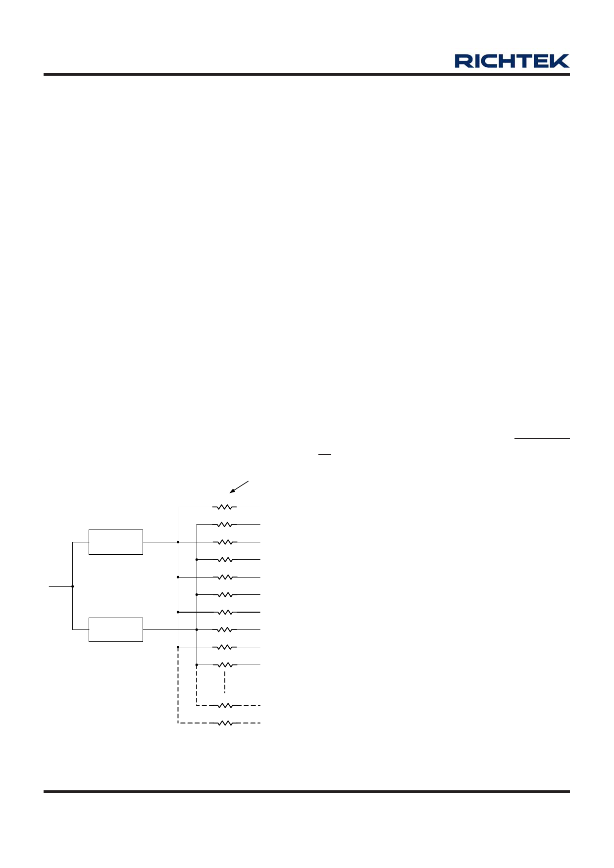
Distributed Bus Terminating Topology
RT9173/A
VOUT
REFEN
RT9173/A
VOUT
Terminator Resistor
R0
BUS(0)
R1
BUS(1)
R2
BUS(2)
R3
BUS(3)
R4
BUS(4)
R5
BUS(5)
R6
BUS(6)
R7
BUS(7)
R8
BUS(8)
R9
BUS(9)
RN
RN+1
BUS(N)
BUS(N+1)
Thermal Consideration
RT9173/A regulators have internal thermal limiting circuitry
designed to protect the device during overload conditions.
For continued operation, do not exceed absolute maximum
operation junction temperature 125°C. The power
dissipation definition in device is :
PD = (VIN - VOUT) x IOUT + VIN x IQ
The maximum power dissipation depends on the thermal
resistance of IC package, PCB layout, the rate of
surroundings airflow and temperature difference between
junction to ambient. The maximum power dissipation can
be calculated by following formula :
PD(MAX) = ( TJ(MAX) -TA ) /θJA
Where TJ(MAX) is the maximum operation junction
temperature 125°C, TA is the ambient temperature and the
θJA is the junction to ambient thermal resistance. The
junction to ambient thermal resistance θJA highly depends
on IC package, PCB layout, and the rate of surroundings
airflow. θJA for SOP-8 package is 160°C/W and TO-263-5
package is 52°C/W on standard JEDEC 51-3 (single layer,
1S) thermal test board. The maximum power dissipation
at TA = 25°C can be calculated by following
formula :
PD(MAX) = (125°C - 25°C) / (160 °C/W)= 0.625W (SOP-8
package)
PD(MAX) = (125°C- 25°C) / (52 °C/W)= 1.923W (TO- 263-
5 package )
Since the multiple VCTRL pins of the SOP-8 package are
internally fused and connected to lead frame, it is efficient
to dissipate the heat by adding cooper area on VCTRL
footprint. Figure 7 shows the package sectional drawing
of SOP-8. Every package has several thermal dissipation
paths, as show in Figure 8, the thermal resistance
equivalent circuit of SOP-8. The path 2 is the main path of
thermal flow due to these materials thermal conductivity.
We define the center of multiple VCTRL pins are the case
point of the path 2.
Figure 6
www.richtek.com
8
DS9173/A-18 March 2007
Share Link: 