RT9259 Ver la hoja de datos (PDF) - Richtek Technology
Número de pieza
componentes Descripción
Lista de partido
RT9259 Datasheet PDF : 15 Pages
| |||
RT9259
The ESR zero is contributed by the ESR associated with
the output capacitance. Note that this requires that the
output capacitor should have enough ESR to satisfy stability
requirements. The ESR zero of the output capacitor
expressed as follows :
fESR
=
2π
1
× COUT
× ESR
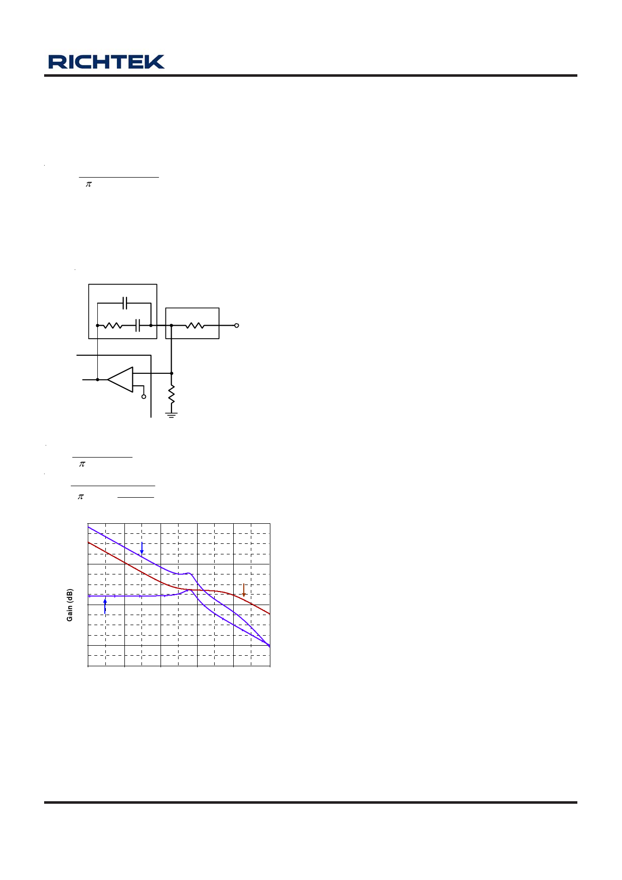
2) Compensation Frequency Equations
The compensation network consists of the error amplifier
and the impedance networks ZC and ZF as shown in
Figure 9.
ZF
C1
R2 C2
ZC
R1
VOUT
- FB
COMP EA+
VREF
RF
Figure 9. Compensation Loop
fZ1
=
2π
1
x R2
x
C2
fP1
=
2π
x R2
1
x
C1 x
C1 +
C2
C2
80 80
Loop Gain
60
40 40
Compensation
Gain
20
00
Modulator
-20 Gain
-40-40
-60-60
110H0zvdb(vo) vdb(comp2)11000vHd0zb(lo)
11.0kKHz
110K0Hzk
FrequFreequnenccyy (Hz)
11000K0Hzk
Figure 10. Bode Plot
1.01MHMz
Figure 10 shows the DC-DC converter's gain vs. frequency.
The compensation gain uses external impedance networks
ZC and ZF to provide a stable, high bandwidth loop. High
crossover frequency is desirable for fast transient response,
but often jeopardize the system stability. In order to cancel
one of the LC filter poles, place the zero before the LC
filter resonant frequency. In the experience, place the zero
at 75% LC filter resonant frequency. Crossover frequency
should be higher than the ESR zero but less than 1/5 of
the switching frequency. The second pole is placed at half
the switching frequency.
Thermal Considerations
For continuous operation, do not exceed absolute
maximum operation junction temperature 125°C. The
maximum power dissipation depends on the thermal
resistance of IC package, PCB layout, the rate of
surroundings airflow and temperature difference between
junction to ambient. The maximum power dissipation can
be calculated by following formula :
PD(MAX) = ( TJ(MAX) − TA ) / θJA
Where TJ(MAX) is the maximum operation junction
temperature 125°C, TA is the ambient temperature and the
θJA is the junction to ambient thermal resistance.
For recommended operating conditions specification of
RT9259, where TJ(MAX) is the maximum junction
temperature of the die (125°C) and TA is the maximum
ambient temperature. The junction to ambient thermal
resistance θJA is layout dependent. For VQFN-16L 4x4
packages, the thermal resistance θJA is 54°C/W on the
standard JEDEC 51-7 four-layers thermal test board.
The maximum power dissipation at TA = 25°C can be
calculated by following formula :
PD(MAX) = ( 125°C − 25°C ) / 54°C/W = 1.852 W for
QFN-16L 4x4 packages
PD(MAX) = ( 125°C − 25°C) / 100°C/W = 1.000 W for
SOP-14 packages
PD(MAX) = ( 125°C − 25°C ) / 110°C/W = 0.909 W for
SSOP-16 packages
The maximum power dissipation depends on operating
ambient temperature for fixed TJ (MAX) and thermal resistance
θJA. For RT9259 packages, the Figure 11 of derating curves
allows the designer to see the effect of rising ambient
temperature on the maximum power allowed.
DS9259-03T00 August 2007
www.richtek.com
11
Share Link: 