RT9261B Ver la hoja de datos (PDF) - Richtek Technology
Número de pieza
componentes Descripción
Lista de partido
RT9261B Datasheet PDF : 8 Pages
| |||
Preliminary
RT9261B
Absolute Maximum Ratings
z Output Voltage -------------------------------------------------------------------------------------------------------- 8V
z LX Pin Voltage --------------------------------------------------------------------------------------------------------- 8V
z EN Pin Voltage(1) ------------------------------------------------------------------------------------------------------ −0.3 to VOUT +0.3V
z LX Pin Output Current ----------------------------------------------------------------------------------------------- 400mA
z Power Dissipation, PD @ TA = 25°C
SOT-89 ------------------------------------------------------------------------------------------------------------------ 0.5W
SOT-23-5 --------------------------------------------------------------------------------------------------------------- 0.25W
z Package Thermal Resistance
SOT-89, θJC ------------------------------------------------------------------------------------------------------------ 100° C/W
SOT-89, θJA ------------------------------------------------------------------------------------------------------------ 300° C/W
SOT-23-5, θJA ---------------------------------------------------------------------------------------------------------- 250° C/W
z Operating Temperature Range ------------------------------------------------------------------------------------- −20 to +85°C
z Storage Temperature Range --------------------------------------------------------------------------------------- −65°C to 150°C
z Lead Temperature (Soldering, 10 sec.) -------------------------------------------------------------------------- 260°C
Notes: (1) Applicable to RT9261B-xxCB
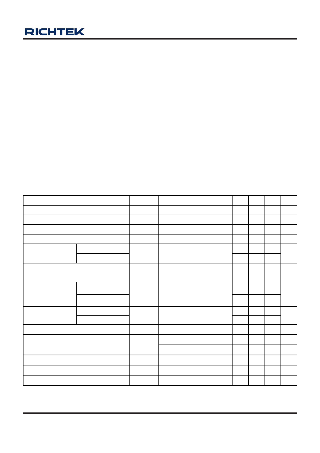
Electrical Characteristics (Refer to Figure 1)
Parameter
Symbol
Test Conditions
Output Voltage Accuracy
ΔVOUT
Input Voltage
VIN
Start-up Voltage
VST
Hold-on Voltage
Input Current 1
VOUT ≤ 3.5V (1)
3.5V < VOUT ≤ 5V (2)
VHO
IOUT = 1mA, VIN: 0 → 2V
IOUT = 1mA, VIN: 2 → 0V
To be measured at VIN in
continuous switching
Input Current 2 (1) (2)
To be measured at VOUT in
switch off condition
Min Typ Max Units
-2 -- +2 %
-- -- 7 V
-- 0.8 1 V
0.7 -- -- V
-- 24 36
μA
-- 36 45
-- 6.5 10 μA
Input Current 3
VOUT ≤ 3.5V (1)
3.5V < VOUT ≤ 5V (2)
To be measured at VIN in no --
load (guaranteed by I1 and I2) --
18 36
μA
20 45
LX Switching Current VOUT ≤ 3.5V (1)
3.5V < VOUT ≤ 5V (2)
ISWITCHING VLX = 0.4V
120 --
160 --
--
mA
--
LX Leakage Current
ILEAKAGE VLX = 6V
-- -- 0.5 μA
Maximum Oscillator Frequency
FMAX
VOUT = 2.5V to 5V
VOUT = 1.5V to 2.4V
140 190 240 kHz
140 190 320 kHz
Oscillator Duty Cycle
DOSC
On (VLX “L”) side
65 75 85 %
Efficiency
-- 80 -- %
VLX Voltage Limit
LX switch on
0.65 0.8 1.0 V
Notes:
(1) VIN = 1.8V, VSS = 0V, IOUT = 1mA, Topt = 25° C, and use External Circuit of Typical Application
(2) VIN = 3V, VSS = 0V, IOUT = 1mA, Topt= 25°C, and External Circuit of Typical Application
DS9261B-12 March 2007
www.richtek.com
3
Share Link: 