S1R72U06 Ver la hoja de datos (PDF) - Seiko Epson Corp
Número de pieza
componentes Descripción
Lista de partido
S1R72U06 Datasheet PDF : 32 Pages
| |||
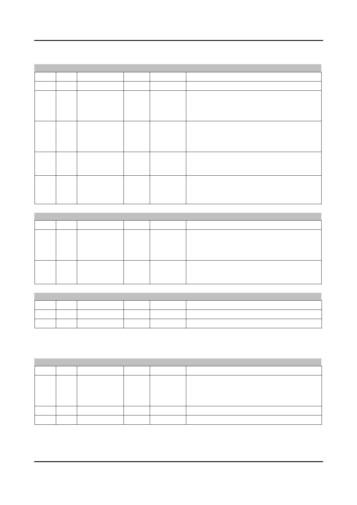
6. Pin Functions
6. Pin Functions
GENERAL (CVDD system)
BGA QFP
Name
-
29 XRESET
-
39 CLKSEL
-
41 CLK_Source
-
40 CLKIN
-
42 CLKOUT
I/O
IN
IN
IN
IN
OUT
RESET
-
-
-
-
Low
Pin description
Reset signal
Clock frequency selection
Set the frequency input from the clock source (CLKIN
or XI pin).
1: 24 MHz 0: 12 MHz
Clock source selection
Set whether the clock source is input from the CLKIN
or XI pin.
1: CLKIN 0: XI
Clock input
12 MHz / 24MHz
If the clock input is from the XI pin, set this pin to Low.
Clock output
Refer to the S1R72U06 Technical Manual for
information on how to change the clock output.
48 MHz / 24 MHz / 12 MHz / 6 MHz / 3 MHz / STOP
OSC (LVDD system)
BGA QFP
Name
-
10 XI
-
11 XO
I/O
IN
OUT
RESET
-
-
Pin description
Internal oscillator circuit input
If the clock input is from the CLKIN pin, set this pin to
Low.
12 MHz / 24 MHz
Internal oscillator circuit output
If the clock input is from the CLKIN pin, leave this pin
open.
TEST (LVDD, CVDD systems)
BGA QFP
Name
-
44 TSTEN
-
37 ATPGEN
I/O
IN(PD)
IN(PD)
RESET
-
-
Pin description
Test pin (*1); not intended for use by user
Test pin (*1); not intended for use by user
PD: Pull-down I/Os are used.
*1 This is pulled down inside the LSI. However, we recommend fixing it at Low on the circuit board.
USB (UVDD3 system)
BGA QFP
Name
-
9 VBUS
-
8 DP
-
7 DM
I/O
IN
BI
BI
RESET
-
Hi-Z
Hi-Z
Pin description
VBUS input pin
VBUS input pin when S1R72U06 is used as USB
device. Leave this pin open when using S1R72U06
as a USB host.
USB data line Data+
USB data line Data-
S1R72U06 Data Sheet
Seiko Epson Corporation
7
(Rev. 1.10)
Share Link: 