SC1563IMS Ver la hoja de datos (PDF) - Semtech Corporation
Número de pieza
componentes Descripción
Lista de partido
SC1563IMS Datasheet PDF : 8 Pages
| |||
VERY LOW DROPOUT, LOW
QUIESCENT 500mA REGULATOR
SC1563
PRELIMINARY - September 11, 2000
APPLICATIONS INFORMATION
Introduction
The SC1563 is intended for applications such as
graphics cards where high current capability and very
low dropout voltage are required. It provides a very
simple, low cost solution that uses little pcb real estate
and typically does not require a heatsink. Additional
features include an enable pin to allow for a very low
power consumption standby mode, and a fully ad-
justable output.
Component Selection
Input capacitor - a 1µF ceramic capacitor is recom-
mended. This allows for the device being some dis-
tance from any bulk capacitance on the rail. Addition-
ally, input droop due to load transients is reduced, im-
proving load transient response. Additional capaci-
tance may be added if required by the application.
Output capacitor - a minimum bulk capacitance of 1µF,
along with a 0.1µF ceramic decoupling capacitor is rec-
ommended. Increasing the bulk capacitance will im-
prove the overall transient response. The use of multi-
ple lower value ceramic capacitors in parallel to
achieve the desired bulk capacitance will not cause
stability issues. Although designed for use with ce-
ramic output capacitors, the SC1563 is extremely toler-
ant of output capacitor ESR values and thus will also
work comfortably with tantalum output capacitors.
External voltage selection resistors - the use of 1% re-
sistors, and designing for a current flow ≥ 10µA is rec-
ommended to ensure a well regulated output (thus R2
≤ 120kΩ).
Thermal Considerations
The power dissipation in the SC1563 is approximately
equal to the product of the output current and the input
to output voltage differential:
PD ≈ (VIN − VOUT ) • IO
The absolute worst-case dissipation is given by:
( ) PD (MAX ) = VIN (MAX ) − VOUT (MIN ) • IO (MAX ) + VIN (MAX ) • IQ (MAX )
For a typical scenario, VIN = 3.3V ± 5%, VOUT = 2.5V
and IO = 500mA, therefore:
VIN(MAX) = 3.465V, VOUT(MIN) = 2.450V and
IQ(MAX) = 1.75mA,
Thus PD(MAX) = 0.514W.
Using this figure, and assuming TA(MAX) = 85°C, we can
calculate the maximum thermal impedance allowable
to maintain TJ ≤ 150°C:
( ) ( ) R = TH(J−A )(MAX )
TJ(MAX ) − TA (MAX )
PD(MAX )
=
150 − 70
0.514
= 156 °C / W
This should be achievable using pcb copper area to aid
in conducting the heat away from the device. Internal
ground/power planes and air flow will also assist in re-
moving heat. For higher ambient temperatures addi-
tional board copper may be required. Use of the avail-
able MSOP-8 package will allow operation at full load
where higher input to output voltage differentials exist.
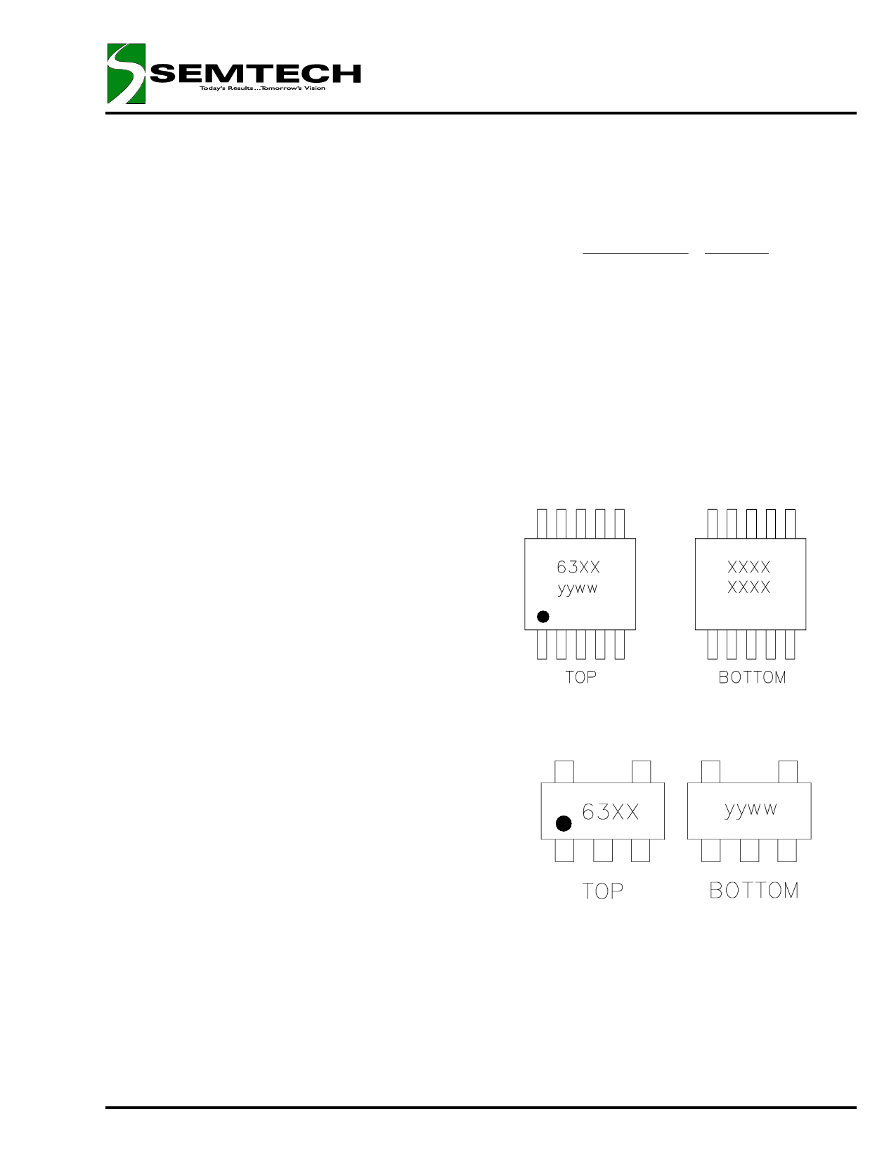
MARKING INFORMATION
MSOP-8
SOT-23-5L
63XX = SC1563, voltage option (example: 6318)
yyww = Datecode (example: 0008)
XXXX = Lot number (example: E01102)
© 2000 SEMTECH CORP.
6
652 MITCHELL ROAD NEWBURY PARK CA 91320
Share Link: 