SC16315S Ver la hoja de datos (PDF) - Silan Microelectronics
Número de pieza
componentes Descripción
Lista de partido
SC16315S Datasheet PDF : 12 Pages
| |||
SC16315S
(Continued)
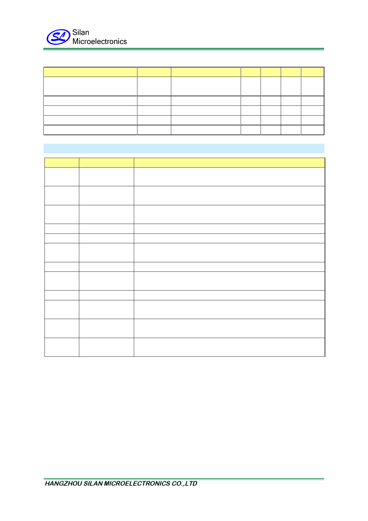
Characteristic
High-Level Input Voltage
Low-Level Input Voltage
Oscillation Frequency
Input Current
Dynamic Current Consumption
PIN DESCRIPTION
Pin No.
Pin Name
1
CLK
2
STB
3, 4
5, 25
6, 24
7~14
15
16~19
20~23
26
K1 to K2
VSS
VDD
SG1/KS1 to
SG8/KS8
VEE
SG9/GR8 to
SG12/GR5
GR4 to GR1
OSC
27
DOUT
28
DIN
Symbol
Test conditions
VIH
--
VIL
fosc
II
IDDdyn
--
R=100KΩ
VI=VDD or VSS
Under no load, display off
Min.
0.7
VDD
VSS
350
--
--
Typ. Max. Unit
-- VDD
V
-- 0.3VDD V
500 650 kHz
--
±1
µA
--
3
mA
Description
Clock input pin. This pin reads serial data at the rising edge and outputs
data at the falling edge.
Serial interface strobe pin. The data input after the STB has fallen is
processed as a command. When this pin is”HIGH”, CLK is ignored.
Key data input pins. At the end of the display cycle, the data sent to these
pins are latched.
Logic ground pin
Logic power supply
High voltage segment output pins also acts as the key source.
Pull down level.
High voltage segment/Grid output pins.
High voltage Gird output pins
Oscillator input pin. Determining the oscillation frequency by a resistor
which is connected to this pin and GND (VSS).
Data output pin (N-channel, open drain) this pin outputs serial data at the
falling edge of the shift clock (starting from the lower bit).
Data input pin. This pin inputs serial data at the rising edge of the shift
clock (starting from the lower bits).
HANGZHOU SILAN MICROELECTRONICS CO.,LTD
Http: www.silan.com.cn
REV:1.2 2004.03.01
Page 3 of 13
Share Link: 