CS8427-IS Ver la hoja de datos (PDF) - Cirrus Logic
Número de pieza
componentes Descripción
Lista de partido
CS8427-IS Datasheet PDF : 59 Pages
| |||
CS8427
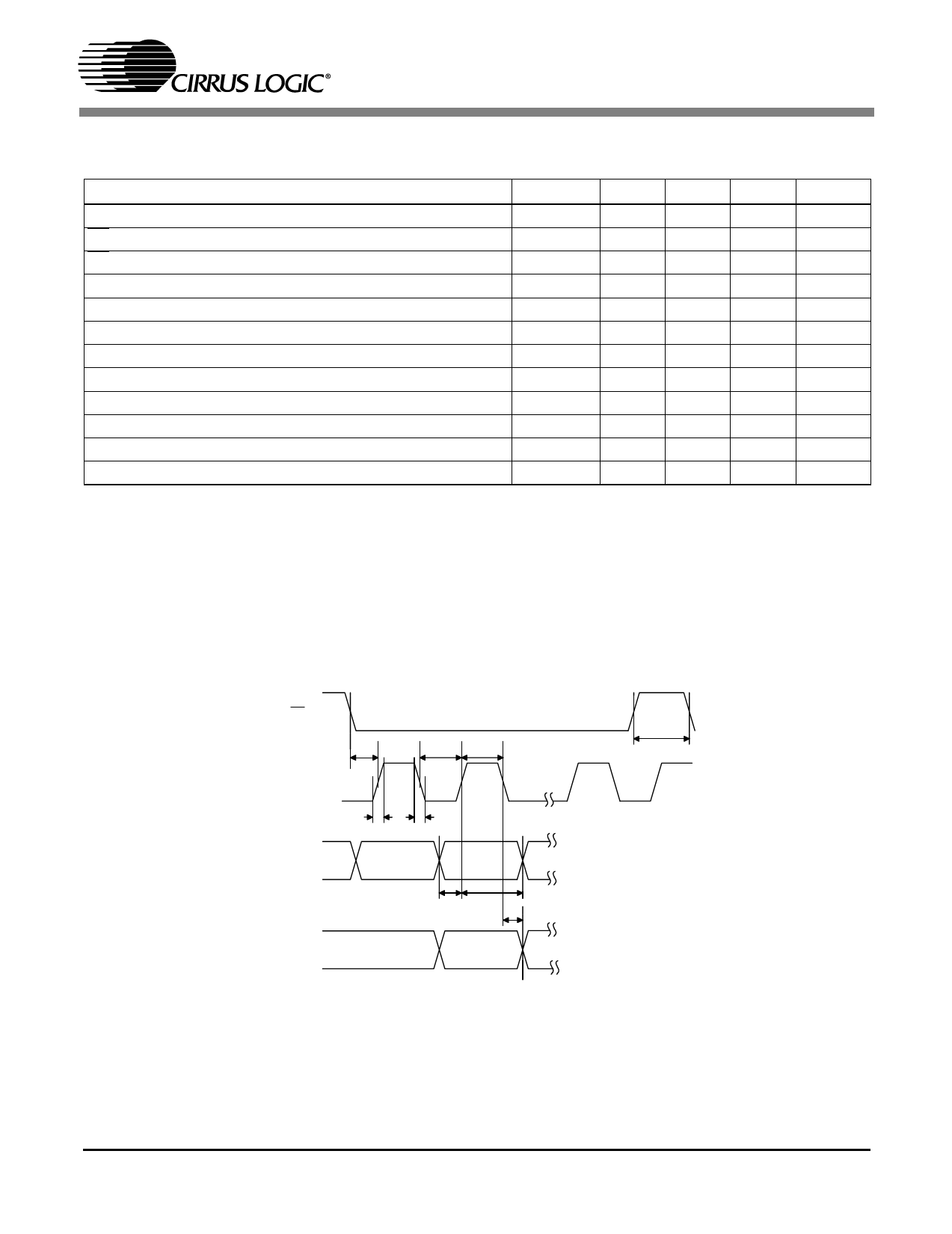
SWITCHING CHARACTERISTICS - CONTROL PORT - SPI MODE
(Inputs: Logic 0 = 0 V, Logic 1 = VL+; CL = 20 pF)
Parameter
Symbol Min Typ Max
CCLK Clock Frequency
CS High Time Between Transmissions
CS Falling to CCLK Edge
CCLK Low Time
CCLK High Time
CDIN to CCLK Rising Setup Time
CCLK Rising to DATA Hold Time
CCLK Falling to CDOUT Stable
Rise Time of CDOUT
Fall Time of CDOUT
Rise Time of CCLK and CDIN
Fall Time of CCLK and CDIN
(Note 14)
fsck
0
-
6.0
tcsh
1.0
-
-
tcss
20
-
-
tscl
66
-
-
tsch
66
-
-
tdsu
40
-
-
(Note 15)
tdh
15
-
-
tpd
-
-
50
tr1
-
-
25
tf1
-
-
25
(Note 16)
tr2
-
-
100
(Note 16)
tf2
-
-
100
Units
MHz
µs
ns
ns
ns
ns
ns
ns
ns
ns
ns
ns
Notes: 14. If Fso or Fsi is lower than 46.875 kHz, the maximum CCLK frequency should be less than 128 Fso and
less than 128 Fsi. This is dictated by the timing requirements necessary to access the Channel Status
and User Bit buffer memory. Access to the control register file can be carried out at the full 6 MHz rate.
The minimum allowable input sample rate is 8 kHz, so choosing CCLK to be less than or equal to
1.024 MHz should be safe for all possible conditions.
15. Data must be held for sufficient time to bridge the transition time of CCLK.
16. For fsck < 1 MHz.
CS
t css
CCLK
t r2
CDIN
CDOUT
t scl t sch
t f2
t dsu
t dh
t pd
t csh
Figure 3. SPI Mode timing
DS477F1
9
Share Link: 