SL610 Ver la hoja de datos (PDF) - Zarlink Semiconductor Inc
Número de pieza
componentes Descripción
Lista de partido
SL610 Datasheet PDF : 7 Pages
| |||
SL610/611 & 612
ELECTRICAL CHARACTERISTICS
These characteristics are guaranteed over the following conditions (unless otherwise stated)
Supply voltage VCC: 6V
Ambient temperature: 22°C ± 2°C
Test frequency: SL610C 30MHz
SL611C 30MHz
SL612C 1.75MHz
Characteristics
Supply current
Voltage gain
Cut-off frequency (-3dB)
Max. output signal (max. AGC)
Max.input signal (max. AGC)
AGC range
AGC current
Circuit
SL610C
SL611C
SL612C
SL610C
SL611C
SL612C
SL610C
SL611C
SL612C
SL610C
SL611C
SL612C
Min.
18
24
32
85
50
10
Value
Typ.
15
15
3.3
20
26
34
120
80
15
1.0
Max.
20
20
5
22
28
36
Units
mA
mA
mA
dB
dB
dB
MHz
MHz
MHz
V rms
250
mV rms
40
50
dB
40
50
dB
60
70
dB
0.15 0.6
mA
Conditions
No signal, Pin 3 open circuit
RS = 50Ω
RL = 22°C
Tamb = 22°C
RL = 150Ω (SL610C/611C)
RL = 1.2kΩ (SL612C)
Pin 7 0V to 5.1V
Current into pin 7 at 5.1V
APPLICATION NOTES
Input circuit
The SL610C, SL611C and SL612C are normally used with
pins 5 and 6 connected together and with the input connected
via a capacitor as shown in Fig.2.
The input impedance is negative between 30MHz and
100MHz (SL610C, SL611C only) and is shown in Fig.3. The
source and inductive is should be shunted by a 1kΩ resistor to
prevent oscillation.
An alternative circuit with improved noise figure is shown in
Fig.4.
AGC
When pin 7 is open circuit or connected to a voltage less
than 2V the voltage gain is normal. As the AGC voltage is
increased there is a reduction in gain as shown in Fig.6. This
reduction varies with temperature.
5
6
4
3
8
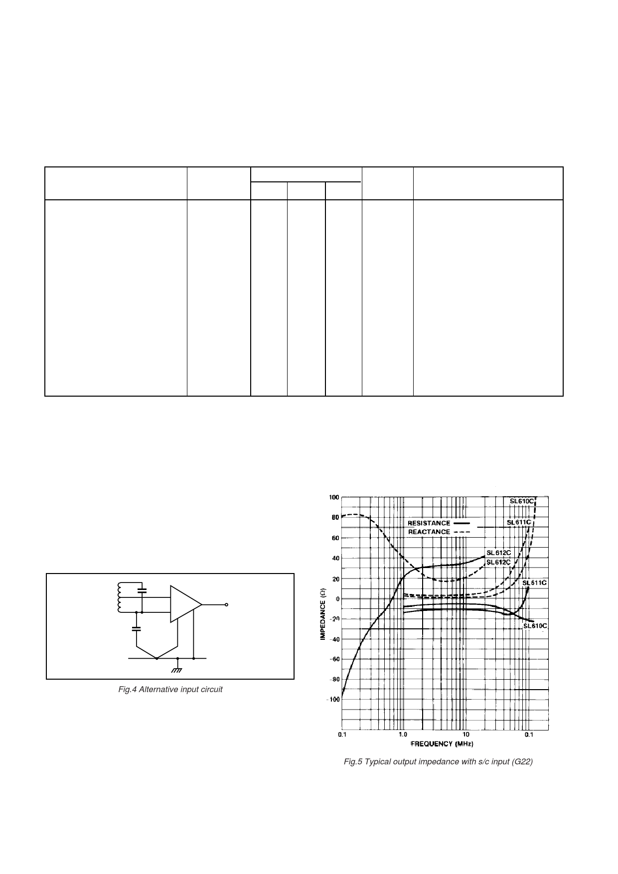
Fig.4 Alternative input circuit
Output circuit
The output stage is an emitter follower and has a negative
output impedance at certain frequencies as shown in Fig.5.
To prevent oscillation when the load is capacitive a 47Ω
resistor should be conncted in series with the output.
Fig.5 Typical output impedance with s/c input (G22)
Share Link: 