IMISM561BZ Ver la hoja de datos (PDF) - Cypress Semiconductor
Número de pieza
componentes Descripción
Lista de partido
IMISM561BZ Datasheet PDF : 8 Pages
| |||
SM561
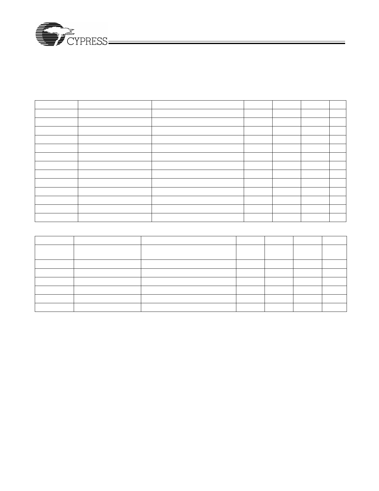
Absolute Maximum Ratings[1]
Supply Voltage (VDD): .................................... –0.5V to +6.0V
DC Input Voltage:...................................–0.5V to VDD + 0.5V
Junction Temperature .................................–40°C to +140°C
Operating Temperature:...................................... 0°C to 70°C
Storage Temperature .................................. –65°C to +150°C
Static Discharge Voltage(ESD)........................... 2,000V–Min
DC Electrical Characteristics (VDD = 3.3V, Temp. = 25°C and CL (pin 4) = 15 pF, unless otherwise noted)
Parameter
Description
Conditions
Min.
Typ.
Max. Unit
VDD
Power Supply Range
± 10%
2.97
3.3
3.63
V
VINH
VINM
VINL
VOH1
VOH2
VOL1
VOL2
Cin1
Input High Voltage
Input Middle Voltage
Input Low Voltage
Output High Voltage
Output High Voltage
Output Low Voltage
Output Low Voltage
Input Capacitance
S0 and S1 only
S0 and S1 only
S0 and S1 only
IOH = 6 ma
IOH = 20 ma
IOH = 6 ma
IOH = 20 ma
Xin/CLK (pin 1)
0.85VDD
VDD
VDD
V
0.40VDD 0.50VDD 0.60VDD V
0.0
0.0
0.15VDD V
2.4
V
2.0
V
0.4
V
1.2
V
3
4
5
pF
Cin2
Input Capacitance
Xout (pin 8)
6
8
10
pF
Cin2
Input Capacitance
S0, S1, SSCC (pins 7, 6, 5)
3
4
5
pF
IDD1
Power Supply Current
FIN = 65 MHz
35
45
mA
IDD2
Power Supply Current
FIN = 166 MHz
50
55
mA
Electrical Timing Characteristics (VDD = 3.3V, T = 25°C and CL=15 pF, unless otherwise noted)
Parameter
Description
Conditions
Min.
Typ.
Max.
ICLKFR
Input Clock Frequency
Range
VDD = 3.30V
54
166
Trise
Clock Rise Time (pin 4) SSCLK1 @ 0.4 – 2.4V
1.2
1.4
1.6
Tfall
Clock Fall Time (pin 4) SSCLK1 @ 0.4 – 2.4V
1.2
1.4
1.6
DTYin
Input Clock Duty Cycle XIN/CLK (pin 1)
20
50
80
DTYout
Output Clock Duty Cycle SSCLK1 (pin 4)
45
50
55
JCC1
Cycle-to-Cycle Jitter
Fin = 140 MHz
–
125
175
JCC2
Cycle-to-Cycle Jitter
Fin = 140 MHz
–
150
200
Note:
1. Single Power Supply: The Voltage on any input or I/O pin cannot exceed the power pin during power up.
Unit
MHz
ns
ns
%
%
ps
ps
Document #: 38-07021 Rev. *C
Page 4 of 8
Share Link: 