HIP6019 Ver la hoja de datos (PDF) - Intersil
Número de pieza
componentes Descripción
Lista de partido
HIP6019 Datasheet PDF : 15 Pages
| |||
HIP6019
OVER-CURRENT TRIP: VDS > VSET
(ID • rDS(ON) > IOCSET • ROCSET)
OCSET
IOCSET
200µA
VCC
DRIVE
UGATE
OC2
+
-
OVER-
CURRENT2
PHASE
PWM
GATE
CONTROL
HIP6019
VIN = +5V
ROCSET
VSET +
ID
+
VDS
VPHASE = VIN - VDS
VOCSET = VIN - VSET
FIGURE 9. OVER-CURRENT DETECTION
Resistors (ROCSET1 and ROCSET2) program the over-
current trip levels for each PWM converter. As shown in
Figure 9, the internal 200µA current sink develops a voltage
across ROCSET (VSET) that is referenced to VIN. The DRIVE
signal enables the over-current comparator (OVER-
CURRENT1 or OVER-CURRENT2). When the voltage
across the upper MOSFET (VDS) exceeds VSET, the over-
current comparator trips to set the over-current latch. Both
VSET and VDS are referenced to VIN and a small capacitor
across ROCSET helps VOCSET track the variations of VIN due
to MOSFET switching. The over-current function will trip at a
peak inductor current (IPEAK) determined by:
IPEAK = -I-O-----C----S----Er--D--T---S--×--(--O-R---N-O---)--C----S----E----T-
The OC trip point varies with MOSFET’s temperature. To avoid
over-current tripping in the normal operating load range,
determine the ROCSET resistor from the equation above with:
1. The maximum rDS(ON) at the highest junction temperature.
2. The minimum IOCSET from the specification table.
3. Determine IPEAK for IPEAK > IOUT(MAX) + (∆I)/2,
where ∆I is the output inductor ripple current.
For an equation for the output inductor ripple current see
the section under component guidelines titled ‘Output
Inductor Selection’.
OUT1 Voltage Program
The output voltage of the PWM1 converter is programmed to
discrete levels between 1.8VDC and 3.5VDC. This output is
designed to supply the microprocessor core voltage. The
voltage identification (VID) pins program an internal voltage
reference (DACOUT) through a TTL-compatible 5-bit digital-to-
analog converter. The level of DACOUT also sets the PGOOD
and OVP thresholds. Table 1 specifies the DACOUT voltage for
the different combinations of connections on the VID pins. The
VID pins can be left open for a logic 1 input, because they are
internally pulled up to +5V by a 10µA current source. Changing
the VID inputs during operation is not recommended. The
sudden change in the resulting reference voltage could toggle
the PGOOD signal and exercise the over-voltage protection. All
VID pin combinations resulting in an INHIBIT disable the IC and
the open-collector at the PGOOD pin.
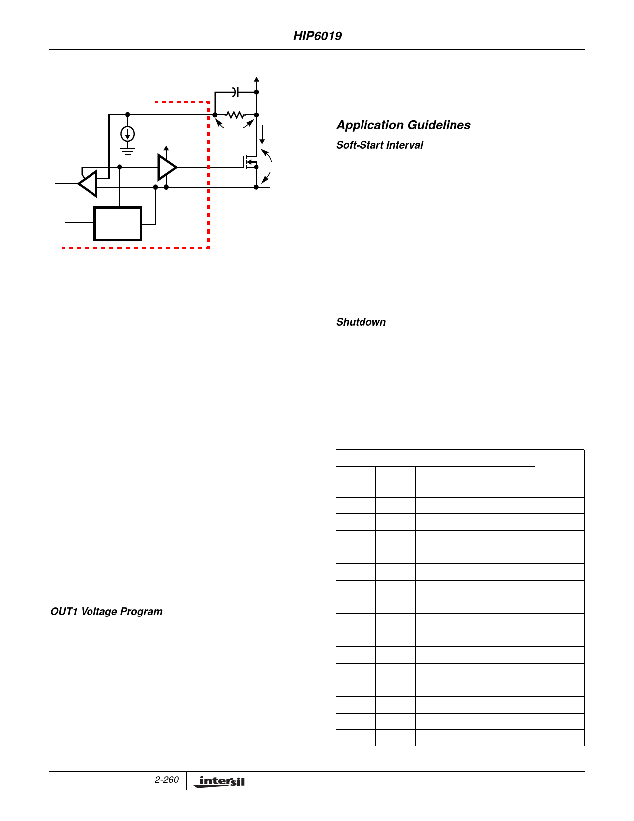
Application Guidelines
Soft-Start Interval
Initially, the soft-start function clamps the error amplifiers’
output of the PWM converters. After the output voltage
increases to approximately 80% of the set value, the
reference input of the error amplifier is clamped to a voltage
proportional to the SS pin voltage. The resulting output
voltage sequence is shown in Figure 6.
The soft-start function controls the output voltage rate of rise
to limit the current surge at start-up. The soft-start interval is
programmed by the soft-start capacitor, CSS. Programming
a faster soft-start interval increases the peak surge current.
The peak surge current occurs during the initial output
voltage rise to 80% of the set value.
Shutdown
Neither PWM output switches until the soft-start voltage
(VSS) exceeds the oscillator’s valley voltage. Additionally, the
reference on each linear’s amplifier is clamped to the soft-
start voltage. Holding the SS pin low (with an open drain or
collector signal) turns off all four regulators.
The VID codes resulting in an INHIBIT as shown in Table 1
also shut down the IC.
VID4
0
0
0
0
0
0
0
0
1
1
1
1
1
1
1
TABLE 1. VOUT1 VOLTAGE PROGRAM
PIN NAME
VID3 VID2 VID1
VID0
NOMINAL
OUT1
VOLTAGE
DACOUT
1
X
X
X
INHIBIT
0
1
1
X
INHIBIT
0
1
0
1
1.80
0
1
0
0
1.85
0
0
1
1
1.90
0
0
1
0
1.95
0
0
0
1
2.00
0
0
0
0
2.05
1
1
1
1
INHIBIT
1
1
1
0
2.1
1
1
0
1
2.2
1
1
0
0
2.3
1
0
1
1
2.4
1
0
1
0
2.5
1
0
0
1
2.6
2-260
Share Link: 