ST162552 Ver la hoja de datos (PDF) - Exar Corporation
Número de pieza
componentes Descripción
Lista de partido
ST162552 Datasheet PDF : 28 Pages
| |||
ST16C2552
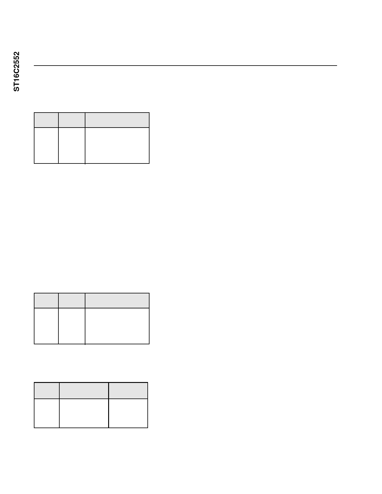
BIT-2 BIT-1
0
0
0
1
1
0
1
1
MF* Function
OP2*
BAUDOUT*
RXRDY*
Reserved
AFR BIT 3-7:
Not used. All these bits are set to logic zero.
LINE CONTROL REGISTER (LCR)
The Line Control Register is used to specify the
asynchronous data communication format. The num-
ber of the word length, stop bits, and parity can be
selected by writing appropriate bits in this register.
LCR BIT1-0:
These two bits specify the word length to be transmit-
ted or received.
BIT-1 BIT-0
0
0
0
1
1
0
1
1
Word length
5
6
7
8
LCR BIT-2:
The number of stop bits can be specified by this bit.
BIT-2 Word length Stop bit(s)
0
5,6,7,8
1
5
1
6,7,8
1
1-1/2
2
LCR BIT-3:
Parity or no parity can be selected via this bit.
0=no parity
1=a parity bit is generated during the transmission,
receiver also checks for received parity.
LCR BIT-4:
If the parity bit is enabled, LCR BIT-4 selects the even
or odd parity format.
0=ODD parity is generated by forcing an odd number
of 1’s in the transmitted data, receiver also checks for
same format.
1= EVEN parity bit is generated by forcing an even
number of 1’s in the transmitted data, receiver also
checks for same format.
LCR BIT-5:
If the parity bit is enabled, LCR BIT-5 selects the
forced parity format.
LCR BIT-5=1 and LCR BIT-4=0, parity bit is forced to
“1” in the transmitted and received data.
LCR BIT-5=1 and LCR BIT-4=1, parity bit is forced to
“0” in the transmitted and received data.
LCR BIT-6:
Break control bit. It causes a break condition to be
transmitted (the TX is forced to low state).
0=normal operating condition.
1=forces the transmitter output (TX) to go low to alert
the communication terminal.
LCR BIT-7:
The internal baud rate counter latch enable (DLAB).
0=normal operation.
1=select Divisor Latch Register and Alternate Func-
tion Register.
MODEM CONTROL REGISTER (MCR)
This register controls the interface with the MODEM
or a peripheral device (RS232).
MCR BIT-0:
0=force DTR* output to high.
1=force DTR* output to low.
MCR BIT-1:
0=force RTS* output to high.
1=force RTS* output to low.
3-144
Share Link: 