TA0030 Ver la hoja de datos (PDF) - RF Micro Devices
Número de pieza
componentes Descripción
Lista de partido
TA0030 Datasheet PDF : 6 Pages
| |||
TA0030
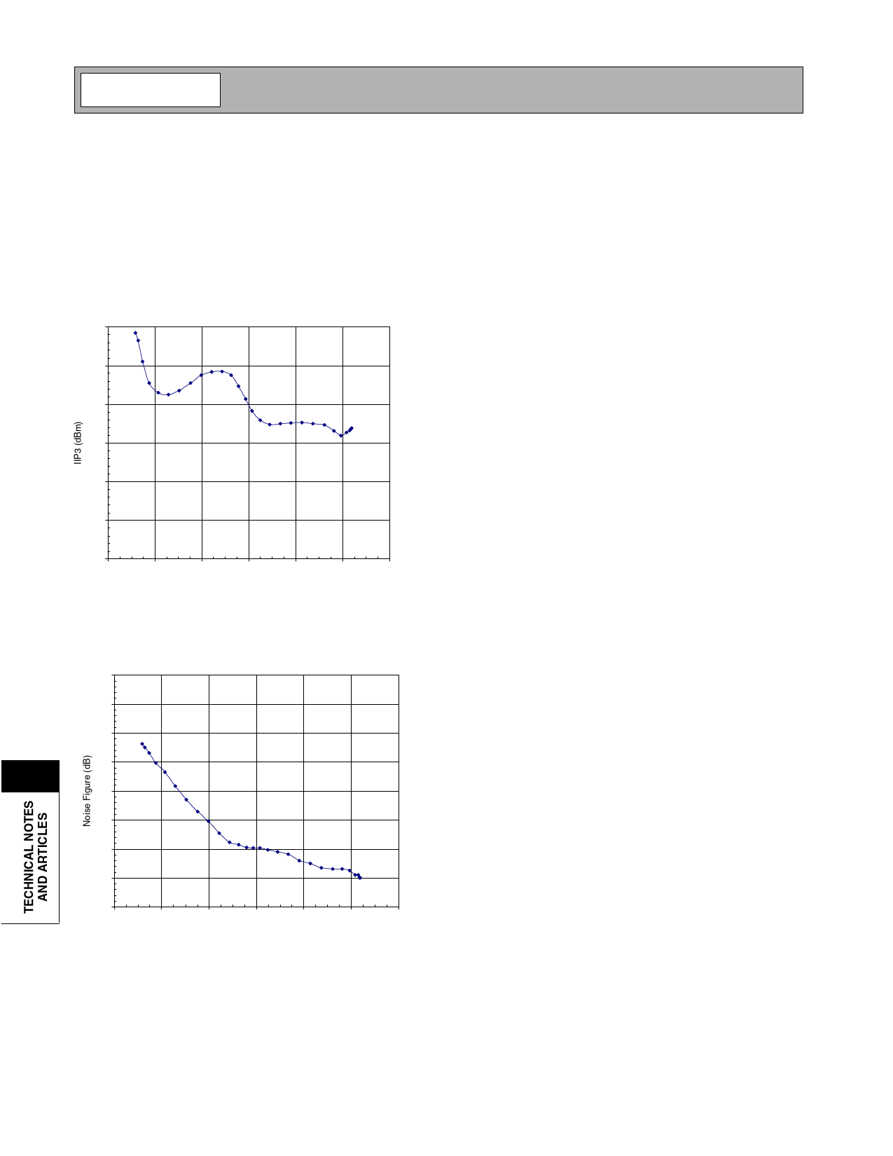
Figure 2) while keeping down the noise figure of the
device (see Figure 3). Although the noise requirements
for the transmit AGC amplifier are not as stringent as
that of the receive AGC amplifier, the challenging IIP3
requirements for the RF2609 make the noise figure
more difficult to achieve. The final design, however,
was able to meet both IS-95 specifications under nomi-
nal and worst-case conditions.
RF2609 IIP3 vs. Gain
(Vcc=3.6 V, 130 MHz)
0
-10
-20
-30
-40
-50
-60
-60
-40
-20
0
20
40
60
Gain (dB)
Figure 2. The RF2609 IIP3 vs. Gain
13
RF2609 Noise Figure vs. Gain
(Vcc=3.6 V, 130 MHz)
80
70
60
50
40
30
20
10
0
-60
-40
-20
0
20
40
60
Gain (dB)
Figure 3. The RF2609 Noise Figure vs. Gain
Understanding how to incorporate the RF2609 into a
transmit chain is straightforward (see Figure 4). Pins 1
and 2 are the input port for the IC.
The differential impedance of the input port is 1000Ω,
so for maximum power transfer, the system designer
need only provide a source impedance of 1000 Ω. Typi-
cally, an intermediate frequency (IF) filter will precede
the RF2609 and provide a 1000Ω source impedance.
If a 1000Ω filter cannot be used, a simple L-C network
can be designed to perform an impedance transforma-
tion. Since there is DC present on pins 1 and 2, the
source should be AC coupled through capacitors as
shown in Figure 4.
Once the IF signal is fed into the IC, it travels through
four variable gain amplifier stages. Each of these
amplifiers is controlled by gain control circuitry, which
primarily consist of operational amplifiers. External to
the part, a DC gain control voltage is fed from a D/A
converter and enters the IC through pin 16. In order to
achieve the correct gain curve, the DC gain control
voltage must pass through a 3.3kΩ resistor. A capaci-
tor is placed from pin 16 to ground in order to lowpass
filter the signal from the D/A converter. The earlier
mentioned gain control voltage range of 0VDC to
3VDC is referenced to the GAIN label on Figure 4, not
at pin 16.
The output port of the RF2609 consists of pins 9 and
10. The output of the IC is open collector, which means
that it looks like a high impedance. Open collector also
means that the output pins must be supplied DC volt-
age externally for the internal output circuitry to oper-
ate.
The output is left high impedance for greater flexibility
and greater precision. A system designer can choose
whatever output impedance they desire and use 1%
resistors to guarantee good matching. The IC was
designed to drive 500Ω (1000Ω output impedance in
parallel with 1000Ω load) but other impedance levels
can be used if the change in power gain is taken into
account. Referring back to Figure 4, a 1000Ω resistor
is placed across pins 9 and 10 to set the differential
output impedance of the IC.
Inductors (L1) connect the power supply to the output
pins. The inductors can be used with series capacitors
(C2) to form an impedance transformation network if
the IF filter does not look like 1000Ω.
If the filter impedance is 1000Ω, then the values of L1
and C1 are chosen to form a parallel-resonant tank cir-
cuit at the signal frequency. In this case, C2 merely
acts as a DC blocking capacitor.
13-152
Copyright 1997-2000 RF Micro Devices, Inc.
Share Link: 