RF2609 Ver la hoja de datos (PDF) - RF Micro Devices
Número de pieza
componentes Descripción
Lista de partido
RF2609 Datasheet PDF : 8 Pages
| |||
RF2609
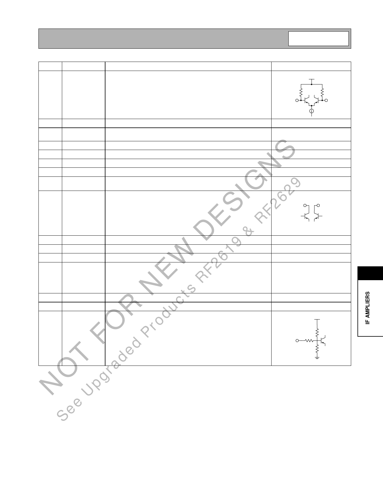
Pin
1
Function
CDMA+
Description
CDMA Balanced Input Pin. This pin is internally DC biased and should
be DC blocked if connected to a device with a DC level, other than VCC,
present. A DC to connection to VCC is acceptable. For single-ended
input operation, one pin is used as an input and the other CDMA input
is AC coupled to ground. The balanced input impedance is 1kΩ, while
the single-ended input impedance is 500Ω.
Interface Schematic
VCC
CDMA+
580 Ω
580 Ω
CDMA-
2
CDMA-
3
GND
4
GND
5
GND
6
GND
7
GND
8
NC
9
OUT-
10
OUT+
11
GND
12
GND
13
VCC
14
VCC
15
VCC
16
GC
NOT
Same as pin 2, except complementary input.
See pin 1 schematic.
Ground connection. Keep traces physically short and connect immedi-
ately to ground plane for best performance.
Same as pin 3.
Same as pin 3.
S Same as pin 3.
Same as pin 3.
N No Connection pin. This pin is internally biased and should not be con-
nected to any external circuitry, including ground or VCC.
G Balanced Output pin. This is an open-collector output, designed to
I operate into a 500Ω balanced load. The load sets the operating imped-
ance, but an external choke or matching inductor to VCC must also be
S supplied in order to correctly bias this output. This bias inductor is typi-
cally incorporated in the matching network between the output and next
stage. Because this pin is biased to VCC, a DC blocking capacitor must
E be used if the next stage’s input has a DC path to ground.
D Same as pin 9, except complementary output.
OUT+
OUT-
See pin 9 schematic.
Same as pin 3.
Same as pin 3.
Supply Voltage pin. External bypassing is required. The trace length
W between the pin and the bypass capacitors should be minimized. The
ground side of the bypass capacitors should connect immediately to
E ground plane. Pins 13, 14, and 15 may share one bypass capacitor if
trace lengths are kept minimal.
N Same as pin 13.
Same as pin 13.
Analog gain adjustment for all amplifiers. Valid control ranges are from
R 0V to 3.0V. Maximum gain is selected with 3.0V. Minimum gain is
selected with 0V. These voltages are valid only for a 3.3kΩ DC source
FOimpedance.
VCC
12.7 kΩ
23.5 kΩ
15 kΩ
10
Rev B3 000822
10-11
Share Link: 