TC5299J Ver la hoja de datos (PDF) - Unspecified
Número de pieza
componentes Descripción
Lista de partido
TC5299J Datasheet PDF : 32 Pages
| |||
TC5299J
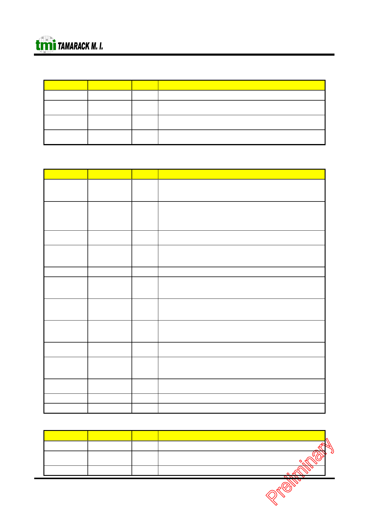
EEPROM/LED Interface Pins
Symbol
Pin #
EECS
73
EESK/LEDLA
72
DO/LEDS
70
DI/LEDF
69
I/O Description
O EEPROM chip select. It is asserted when to access EEPROM.
O Link (on/off) & Receive data (Blink) LED pin. It is also used as a
serial clock for EEPROM data loading.
I/O Speed (100M:ON/10M:OFF) & transmit data (Blink) LED pin. It
is also used as a signal for EEPROM data loading.
O Full-duplex (ON/OFF, Full/Half-duplex) & Collision (Blink)
LED pin. It is a data output pin for EEPROM writing.
External PHY / MII Interface Pins
Symbol
Pin #
I/O
TXD[3:0]
42-43,
O
45-46
TXEN
47
I/O
TXC
RXD[3:0]
RXC
RXDV
RXER
COL
CRS
MDC
MDIO
EXLEDL
EXLEDF
48
I
58-57,
I
55-54
51
I
52
I
50
I
40
I
39
I
59
O
74
I/O
36
I
37
I
Description
Four parallel transmit data lines. This data is synchronized to the
assertion of the TXC signal and is latched by the external PHY
on the rising edge of the TXC signal.
This pin function as transmit enable. It indicates that a
transmission is active on the MII port to an external PHY device.
Pull down this pin on power-on reset to select 50MHz-clock
input from pin X1. Otherwise, use 25MHz-clock input.
Supports the transmit clock supplied by the external PMD device.
This clock should always be active.
Four parallel receive data lines. This data is driven by an external
PHY that attached the media and should be synchronized with
the RXC signal.
Supports receive clock from PHY. And is recovered by the PHY.
Data valid is asserted by an external PHY when receive data is
present on the RXD[3:0] lines and is deasserted at the end of the
packet. This signal should be synchronized with the RXC signal.
Data valid is asserted by an external PHY when receive data is
present on the RXD[3:0] lines and is deasserted at the end of the
packet. This signal should be synchronized with the RXC signal.
This pin functions as the collision detect. When the external
physical layer protocol (PHY) device detects a collision, it asserts
this pin.
In MII mode this pin functions as the carrier sense and is asserted
by the PHY when the media is active.
MII management data clock is sourced by the TC5299J to the
external PHY devices as a timing reference for the transfer of
information on the MDIO signal.
MII management data input/output transfers control information
and status between the external PHY and the TC5299J.
Low active; presents the external PHY link status.
Present the half/full duplex mode for external PHY.
Clock Interface Pins
Symbol
Pin #
X1
66
X2
67
X25M
53
I/O Description
I CRYSTAL OR EXTERNAL OSCILLATOR INPUT: 50 MHz
O CRYSTAL FEEDBACK OUTPUT: used in crystal connection
only.
O 25MHz clock output
-6-
Ver. 0.1
07/04/01
Share Link: 