TC77-5.0MOA Ver la hoja de datos (PDF) - Microchip Technology
Número de pieza
componentes Descripción
Lista de partido
TC77-5.0MOA Datasheet PDF : 22 Pages
| |||
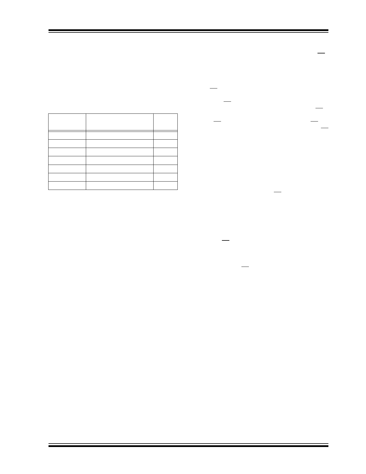
3.1 Temperature Data Format
A 13-bit two’s complement digital word is used to rep-
resent the temperature. The Least Significant Bit (LSb)
is equal to 0.0625°C. Note that the last two LSb bits (Bit
0 and 1) are tri-stated and are represented as a logic ‘1’
in the table. Bit 2 is set to logic ‘1’ after the completion
of the first temperature conversion following a power-
up or voltage reset event.
TABLE 3-1: TC77 OUTPUT
Temperature
Binary
MSB / LSB
Hex
+125°C
+25°C
+0.0625°C
0°C
0011 1110 1000 0111 3E 87h
0000 1100 1000 0111 0B 87h
0000 0000 0000 1111 00 0Fh
0000 0000 0000 0111 00 07h
-0.0625°C
1111 1111 1111 1111 FF FFh
-25°C
1111 0011 1000 0111 F3 87h
-55°C
1110 0100 1000 0111 E4 87h
An over-temperature condition can be determined by
reading only the first few Most Significant Bits (MSb) of
the temperature data. For example, the microprocessor
could read only the first four bits of the Temperature
register in order to determine that an over-temperature
condition exists.
3.2 Power-Up And Power-Down
The TC77 is in the Continuous Temperature Conver-
sion mode at power-up. The first valid temperature con-
version will be available approximately 300 ms (refer to
“Temperature to Bits Converter” section listed in the DC
characteristics table) after power-up. Bit 2 of the Tem-
perature register is set to a logic ‘1’ after the completion
of the first temperature conversion following a power-
up or voltage reset event. Bit 2 is set to logic ‘0’ during
the time needed to complete the first temperature con-
version. Thus, the status of bit 2 can be monitored to
indicate the completion of the first temperature conver-
sion.
A supply voltage lower than 1.6V (typ.) is considered a
power-down state for the TC77. The device will reset
itself and continue its normal Continuous Conversion
mode of operation when the supply voltage rises above
the nominal 1.6V. A minimal supply voltage of 2.7V is
required in order to ensure proper operation of the
device.
TC77
3.3 Serial Bus Interface
The serial interface consists of the Chip Select (CS),
Serial Clock (SCK) and Serial Data (SI/O) signals. The
TC77 meets the SPI and MICROWIRE bus specifica-
tions, with the serial interface designed to be compati-
ble with the Microchip PIC® family of microcontrollers.
The CS input is used to select the TC77 when multiple
devices are connected to the serial clock and data
lines. The CS line is also used to synchronize the data,
which is written to, or read from, the device when CS is
equal to a logic ‘0’ voltage. The SCK input is disabled
when CS is a logic ‘1’. The falling edge of the CS line
initiates communication, while the rising edge of CS
completes the communication.
The SCK input is provided by the external microcon-
troller and is used to synchronize the data on the SI/O
line. The Temperature and Manufacturer ID registers
are read only while the Configuration register is a read/
write register.
Figure 3-2 provides a timing diagram of a read opera-
tion of the Temperature register. Communication with
the TC77 is initiated when the CS goes to a logic ‘0’.
The Serial I/O signal (SI/O) then transmits the first bit of
data. The microcontroller serial I/O bus master clocks
the data in on the rising edge of SCK. The falling edge
of SCK is then used to clock out the rest of the data.
After 14 bits of data (thirteen temperature bits and Bit 2)
have been transmitted, the SI/O line is then tri-stated.
Note that CS can be taken to a logic ‘1’ at any time dur-
ing the data transmission if only a portion of the temper-
ature data information is required. The TC77 will
complete the conversion, and the output shift register
will be updated, if CS goes to the inactive state while in
the middle of a conversion.
Figure 3-3 provides a timing diagram of a multi-byte
communication operation consisting of a read of the
Temperature Data register, followed by a write to the
Configuration register. The first 16 SCK pulses are
used to transmit the TC77's temperature data to the
microcontroller. The second group of 16 SCK pulses
are used to receive the microcontroller command to
place the TC77 either in Shutdown or Continuous Tem-
perature Conversion mode. Note that the TC77 is in the
Continuous Temperature Conversion mode at power-
up.
The data written to the TC77’s Configuration register
should be either all 0’s or all 1’s, corresponding to
either the Continuous Temperature Conversion or
Shutdown mode, respectively. The TC77 is in Shut-
down mode when Bits C0 to C7 are all equal to 1’s. The
TC77 will be in the Continuous Conversion mode if a ‘0’
in any bit location from C0 to C7 is written to the
Configuration register.
2002-2012 Microchip Technology Inc.
DS20092B-page 9
Share Link: 