TDA9901TS Ver la hoja de datos (PDF) - Philips Electronics
Número de pieza
componentes Descripción
Lista de partido
TDA9901TS Datasheet PDF : 20 Pages
| |||
Philips Semiconductors
Wideband differential digital controlled
variable gain amplifier
Product specification
TDA9901
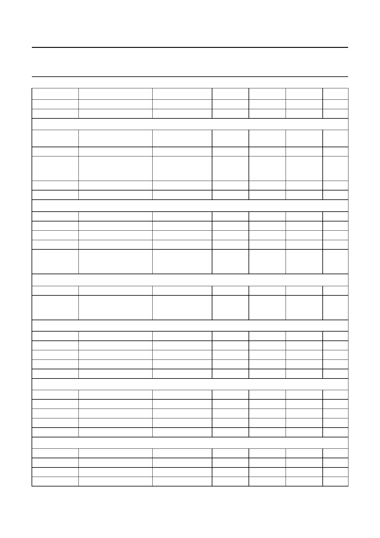
SYMBOL
PARAMETER
CONDITIONS
MIN.
TYP.
MAX.
UNIT
Io(CMADC)(max) maximum output current
Co(CMADC)
output capacitance
Reference voltage output VGA: pin CMVGA
−
1.0
−
mA
−
3
−
pF
Vref(CMVGA)
Ro(CMVGA)
VGA reference output
voltage
output resistance
referenced to VDDA;
Tamb = 25 °C
Tamb = 25 °C
VDDA − 2.48 VDDA − 2.30 VDDA − 2.17 V
−
9
20
Ω
∆Vref(CMVGA)/∆T VGA reference output
voltage variation with
temperature
−
1.75
−
mV/°C
Io(CMVGA)(max) maximum output current
−
1.0
−
mA
Co(CMVGA)
output capacitance
−
3
−
pF
Gain switching characteristics (in latched mode); fCLK = 52 MHz; Tamb = 25°C; (see Fig.3)
th
input data hold time
2.0
−
−
ns
tsu
input data set-up time
3.8
−
−
ns
tW
input data pulse width
5.8
−
−
ns
tPD1
propagation delay time
−
4.2
5.9
ns
tset1
gain settling time
10 to 90% full scale −
2.6
3.2
ns
if ±6 dB gain
change; note 3
Gain switching characteristics (in transparent mode); fCLK = 52 MHz; Tamb = 25°C; (see Fig.4)
tPD2
propagation delay time
−
6.7
9.5
ns
tset2
gain settling time
10 to 90% full scale −
5.4
6.9
ns
if ±6 dB gain
change; note 4
Clock timing input: pins CLK and CLKN (see Fig.3)
fCLK(max)
maximum clock frequency
tCPL
clock LOW pulse width
tCPH
clock HIGH pulse width
tr
rise time
tf
fall time
Digital inputs: pins TE, GRAY0, GRAY1 and GRAY2
52
−
−
MHz
4.0
−
−
ns
4.0
−
−
ns
−
4
−
ns
−
4
−
ns
VIL
LOW-level input voltage
VIH
HIGH-level input voltage
IIH
HIGH-level input current
IIL
LOW-level input current
Ci
input capacitance
Clock inputs in TTL mode
0
−
2.0
−
−10
−
−10
−
−
−
0.8
V
VDDD
V
+10
µA
+10
µA
3
pF
VIL
LOW-level input voltage note 5
VIH
HIGH-level input voltage note 5
IIH
HIGH-level input current
IIL
LOW-level input current
0
−
2.0
−
15
−
−40
−
0.8
V
VDDD
V
80
µA
−10
µA
1999 Oct 08
8
Share Link: 