TMC2005-JT Ver la hoja de datos (PDF) - SMSC -> Microchip
Número de pieza
componentes Descripción
Lista de partido
TMC2005-JT Datasheet PDF : 32 Pages
| |||
ARCNET 5 Port HUB Controller
Datasheet
Option Feature for Jitter Filtering
When any RX ports receive the bigger jitter than its allowance, the TMC2005 may fail to receive the data
correctly and the network may be down.. However the below method to escape is effective for the case that a
momentary big jitter occurs under a special condition like an optical transceiver.
1) Big jitter (BJ) mode
The reference phase of the internal DPLL is changed from the first pulse to the second pulse by setting “0” to the big
jitter mode pins (nBJX). This setup is effective for the case that a big jitter occurs when rising up from DC state as
same as when using an optical transceiver with ATC function (refer to complement).
Note: The delay time of the TMC2005 becomes 400nS (at 2.5Mbps) longer than the normal mode. The delay time
limits the maximum cable length and maximum node number.
[Complement] The big jitter may occur in the case of using an optical transceiver, especially an optical receiver that
has an ATC circuit that controls threshold level in proportion to received light strength. The first pulse especially after
long time idle has the big jitter but the second pulse is stabilized.
2) Changing polar of RX port
In order to filter the jitter of edge in one side, it is effective to set reverse to pin SA, SB, SE to change the polarity of
RX port.
Note: Changing the polarity of RX port makes the delay time of the TMC2005 circuit a half bit (200nS) longer than
original 2.5Mbps, and the delay time affects the maximum cable length and maximum node number.
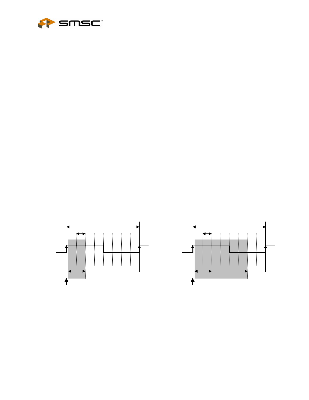
Option Feature for Noise Cut mode
The Noise cut mode is enabled by setting pin nMBx sets 0. The noise cut mode is a function to remove the ringing
noise and the reflection noise generated on the leading edge side of the input pulse to receive data input RXINx. The
position and the width of the “dead band” are shown in the figure below.
- Dead band at Normal mode (nMBx=1)
Period of data rate (Tdr)
Tdr/8 = 1 clock
- Dead band at Noise cut mode (nMBx=0)
Period of data rate (Tdr)
Tdr/8 = 1 clock
RXIN
(Active High)
Ideal waveform
dead band
RXIN edge reference position:
Generated by adjacent phase of SYNC character (1,1,0)
RXIN
(Active High)
Ideal waveform
dead band: Noise cut band
RXIN edge reference position:
Generated by adjacent phase of SYNC character (1,1,0)
SMSC TMC2005-JT
Page 11
DATASHEET
Revision 1.0 (01-30-06)
Share Link: 