TSM1051 Ver la hoja de datos (PDF) - STMicroelectronics
Número de pieza
componentes Descripción
Lista de partido
TSM1051
STMicroelectronics

TSM1051 Datasheet PDF : 15 Pages
| |||
TSM1051
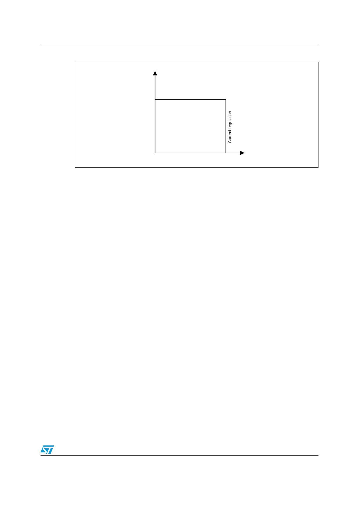
Figure 10. Output voltage versus output current
Vout
Voltage regulation
Application information
Iout (Vcc of the device independent from output voltage)
5.2
Compensation
The voltage-control trans-conductance operational amplifier can be fully compensated. Both
of its output and negative input are directly accessible for external compensation
components.
An example of a suitable compensation network is shown in Figure 3. It consists of a
capacitor Cvc1 = 2.2 nF and a resistor Rcv1 = 470 kΩ in series.
The current-control trans-conductance operational amplifier can be fully compensated. Both
its output and negative input are directly accessible for external compensation components.
An example of a suitable compensation network is shown in Figure 3. It consists of a
capacitor Cic1 = 2.2 nF and a resistor Ric1 = 22 kΩ in series. In order to reduce the
dissipation of the device (especially with VCC voltage values close to 12 V) and to increase
the stability of the application it is suggested to limit the current flowing in the OUT pin of the
device adding a resistor in series with the opto-coupler.
An example of a suitable RLED value could be 330 Ω in series with the opto-coupler in case
VCC = 12 V.
5.3
Start up and short circuit conditions
Under start-up or short-circuit conditions the device is not provided with a high enough
supply voltage. This is due to the fact that the chip has its power supply line in common with
the power supply line of the system.
Therefore, the current limitation can only be ensured by the primary PWM module, which
should be chosen accordingly.
If the primary current limitation is considered not to be precise enough for the application,
then a sufficient supply for the device has to be ensured under any condition. It would then
be necessary to add some circuitry to supply the chip with a separate power line. This can
be achieved in numerous ways, including an additional winding on the transformer.
The following schematic shows how to realize a low-cost power supply for the device (with
no additional windings).
9/15
Share Link: