UBA1707 Ver la hoja de datos (PDF) - Philips Electronics
Número de pieza
componentes Descripción
Lista de partido
UBA1707 Datasheet PDF : 36 Pages
| |||
Philips Semiconductors
Cordless telephone, answering machine
line interface
Product specification
UBA1707
The EHI input can also be used for pulse dialling or
register recall (timed loop break). During line breaks
(voltage at pin EHI is LOW or open-circuit), the voltage
regulator is switched off and the capacitor at pin REG is
internally disconnected to prevent its discharge. As a
result, the voltage stabilizer will have negligible switch-on
delay after line interruptions. This minimizes the
contribution of the IC to the current waveform during pulse
dialling or register recall.
When the UBA1707 is in power-down mode (bit PD at
logic 1), the TPDARL transistor is forced to be turned off
whatever the voltage applied at pin EHI.
SET IMPEDANCE
In the audio frequency range, the dynamic impedance
between pins LN and GND (illustrated in Fig.8) is mainly
determined by the ZSET impedance.
The impedance introduced by the external TNSW transistor
connected between pin GND and the negative line
terminal (LN−) is negligible.
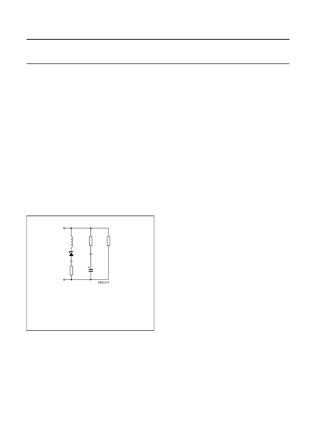
handbook, halfpage LN
LEQ
RP
ZSET
619 Ω
Vref
SLPE
GND
RSLPE
10 Ω
REG
CREG
4.7 µF
MGL215
TRANSMIT AMPLIFIER (PINS TXI+ AND TXI−)
The UBA1707 has symmetrical transmit inputs TXI+ and
TXI−. The input impedance between pins TXI+ or TXI− and
GND is 21 kΩ. The voltage gain from pins TXI+ or TXI− to
pin LN is set at 11.6 dB with 600 Ω line load (Zline) and
619 Ω set impedance. The inputs are biased at
2 × Vd ≅ 1.4 V, with Vd representing the diode voltage.
Automatic gain control is provided on this amplifier for line
loss compensation.
RECEIVE AMPLIFIER (PINS RXI AND RXO; BIT RXM)
The receive amplifier (see Fig.9) has one input (RXI) and
one output (RXO). The input impedance between pins
RXI and GND is 21 kΩ. The rail-to-rail output stage is
designed to drive a 500 µA peak current. The output
impedance at pin RXO is approximately 100 Ω.
The voltage gain from pin RXI to pin RXO is set at 37.9 dB.
This gain value compensates typically the attenuation of
the anti-sidetone network (see Fig.10). The output as well
as the input are biased at 2 × Vd ≅ 1.4 V. Automatic gain
control is provided on this amplifier for line loss
compensation. This amplifier can be muted by activating
the receive mute function (bit RXM at logic 1).
Leq = CREG × RSLPE × RP
RP = internal resistance = 35 kΩ.
Fig.8 Equivalent impedance between
LN and GND.
1999 Feb 17
11
Share Link: 