CS4630-CM Ver la hoja de datos (PDF) - Cirrus Logic
Número de pieza
componentes Descripción
Lista de partido
CS4630-CM Datasheet PDF : 38 Pages
| |||
CS4630
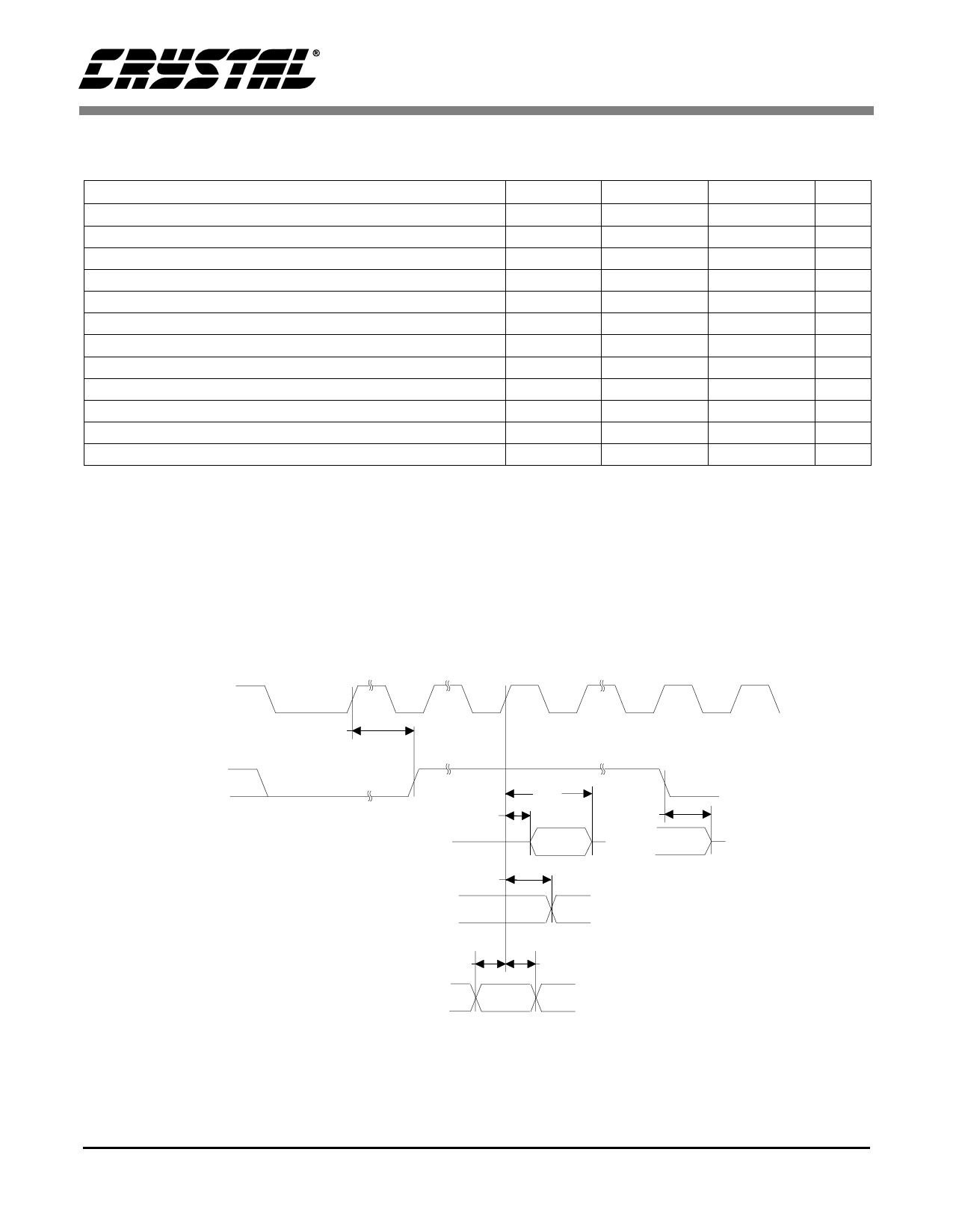
PCI INTERFACE PINS (TA =0° to 70° C; PCIVDD = CRYVDD = 3.3 V; CVDD = 2.5 V; VDD5REF = 5 V;
PCIGND = CGND = CRYGND = 0 V; Logic 0 = 0 V, Logic 1 = 3.3 V; Timing reference levels = 1.4 V)
Parameter
PCICLK cycle time
PCICLK high time
PCICLK low time
PCICLK to signal valid delay - bused signals
(Note 18)
PCICLK to signal valid delay - point to point
(Note 18)
Float to active delay
(Note 15)
Active to Float delay
(Note 15)
Input Set up Time to PCICLK - bused signals (Note 18)
Input Set up Time to PCICLK - point to point
(Note 18)
Input hold time for PCICLK
Reset active time after PCICLK stable
(Note 16)
Reset active to output float delay
(Notes 15, 16, 17)
Symbol
tcyc
thigh
tlow
tval
tval(p+p)
ton
toff
tsu
tsu(p+p)
th
trst-clk
trst-off
Min
30
11
11
2
2
1
-
7
10, 12
0
100
-
Max
Unit
-
ns
-
ns
-
ns
11
ns
12
ns
-
ns
28
ns
-
ns
-
ns
-
ns
-
µs
30
ns
Notes: 15. For Active/Float measurements, the Hi-Z or “off” state is when the total current delivered is less than or
equal to the leakage current. Specification is guaranteed by design, not production tested.
16. RST# is asserted and de-asserted asynchronously with respect to PCICLK.
17. All output drivers are asynchronously floated when RST# is active.
18. REQ# and GNT# are point to point signals. All other PCI signals are considered bused signals.
PCICLK
RST#
t rst-clk
t off
t on
OUTPUTS
Hi-Z
t val
OUTPUTS
Valid
t su
INPUTS
th
Valid
Input
t rst-off
Figure 2. PCI Timing Measurement Conditions
DS445PP1
7
Share Link: 