UPC8129GR Ver la hoja de datos (PDF) - NEC => Renesas Technology
Número de pieza
componentes Descripción
Lista de partido
UPC8129GR
NEC => Renesas Technology

UPC8129GR Datasheet PDF : 28 Pages
| |||
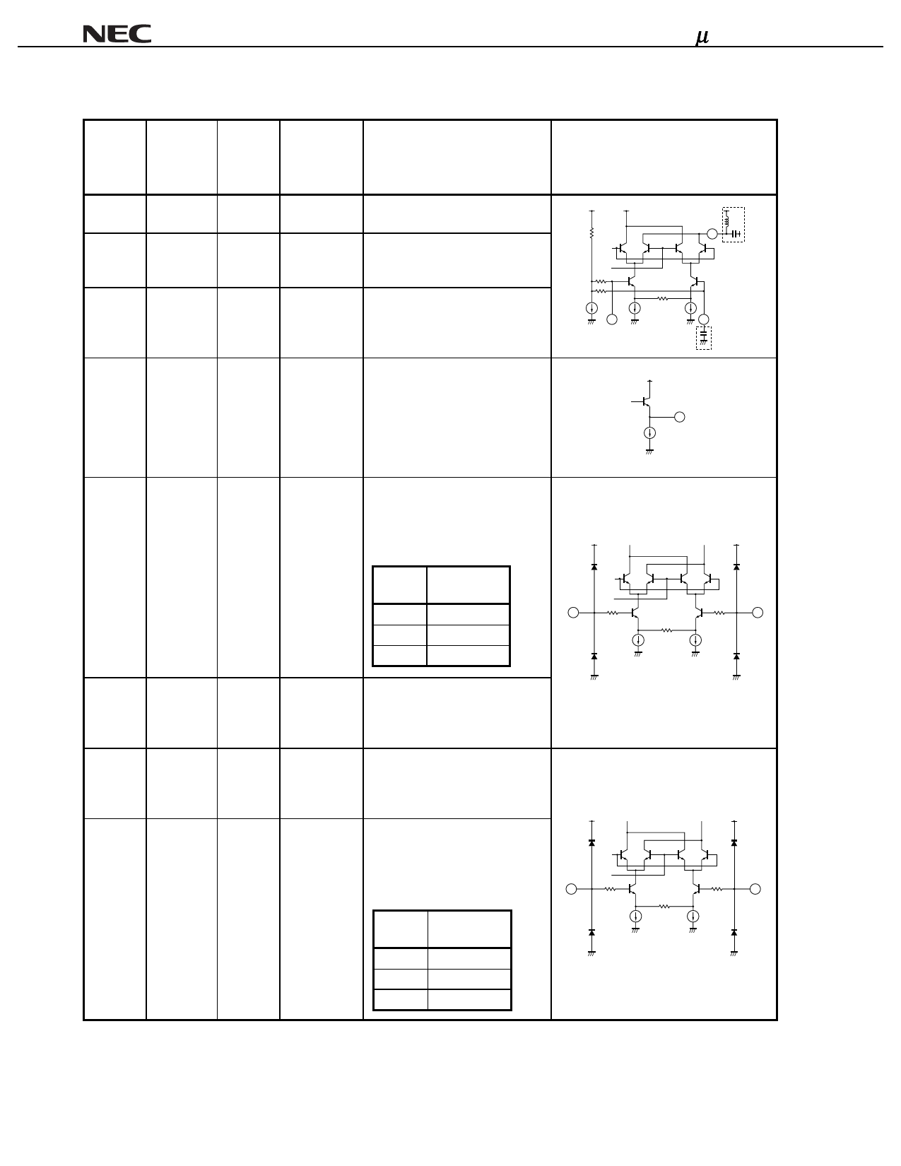
PIN EXPLANATION
Pin No.
18
Symbol
RFout
Supply
Voltage
(V)
VCC
1
UpCon in
–
2
UpCon inb
–
Pin
Voltage
Typ. (V)
@VCC = 3 V
–
2.2
2.2
Description
RF output from Up-Converter.
This pin is open collector output.
IF input for Up-converter.
This pin is high impedance
input.
Bypass of IF input.
Grounded through external
capacitor.
3
MODout
–
1.9
Output from modulator.
This is emitter follower output.
µPC8129GR
Equivalent Circuit
18
1
2
3
4
I
VCC/2
–
Input for I signal. This input
impedance is about 200 kΩ.
Relations between amplitude
and VCC/2 bias of input signal
are following.
VCC/2
(V)
Signal Level Note
(mVP-P)
≥ 1.35
≤ 400
4
5
≥ 1.5
≤ 600
≥ 1.75
≤ 1000
5
Ib
VCC/2
–
Input for I signal. This input
impedance is about 200 kΩ.
VCC/2 biased DC signal should
be input.
6
Qb
VCC/2
–
Input for Q signal. This input
impedance is about 200 kΩ
VCC/2 biased DC signal should
be input.
7
Q
VCC/2
–
Input for Q signal. This input
impedance is about 200 kΩ.
Relations between amplitude
and VCC/2 bias of input signal
are following.
7
6
VCC/2
(V)
≥ 1.35
≥ 1.5
≥ 1.75
Signal Level
(mVP-P)
≤ 400
≤ 600
≤ 1000
Note
Note In the case of that I/Q input signals are single ended.
Of course, I/Q signal inputs can be used either single endedly or differentially with proper terminations.
8
Data Sheet P12781EJ2V0DS00
Share Link: