VN920SP-E Ver la hoja de datos (PDF) - STMicroelectronics
Número de pieza
componentes Descripción
Lista de partido
VN920SP-E Datasheet PDF : 18 Pages
| |||
VN920SP-E
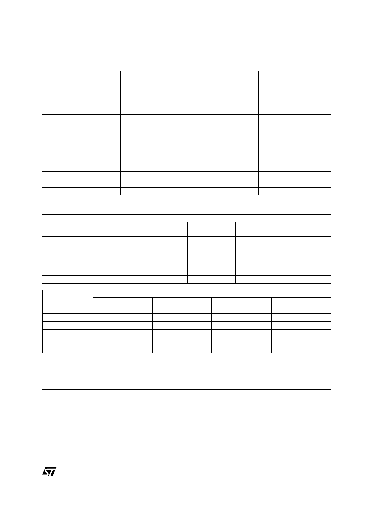
Table 11. Truth Table
CONDITIONS
Normal operation
Overtemperature
Undervoltage
Overvoltage
Short circuit to GND
Short circuit to VCC
Negative output voltage clamp
INPUT
L
H
L
H
L
H
L
H
L
H
H
L
H
L
OUTPUT
L
H
L
L
L
L
L
L
L
L
L
H
H
L
SENSE
0
Nominal
0
VSENSEH
0
0
0
0
0
(Tj<TTSD) 0
(Tj>TTSD) VSENSEH
0
< Nominal
0
Table 12. Electrical Transient Requirements On VCC Pin
ISO T/R 7637/1
Test Pulse
I
TEST LEVELS
II
III
1
-25 V
-50 V
-75 V
2
+25 V
+50 V
+75 V
3a
-25 V
-50 V
-100 V
3b
+25 V
+50 V
+75 V
4
-4 V
-5 V
-6 V
5
+26.5 V
+46.5 V
+66.5 V
IV
-100 V
+100 V
-150 V
+100 V
-7 V
+86.5 V
Delays and
Impedance
2 ms 10 Ω
0.2 ms 10 Ω
0.1 µs 50 Ω
0.1 µs 50 Ω
100 ms, 0.01 Ω
400 ms, 2 Ω
ISO T/R 7637/1
Test Pulse
I
1
C
2
C
3a
C
3b
C
4
C
5
C
TEST LEVELS RESULTS
II
III
IV
C
C
C
C
C
C
C
C
C
C
C
C
C
C
C
E
E
E
CLASS
C
E
CONTENTS
All functions of the device are performed as designed after exposure to disturbance.
One or more functions of the device is not performed as designed after exposure to disturbance
and cannot be returned to proper operation without replacing the device.
7/18
Share Link: 