25X40BLSIG Ver la hoja de datos (PDF) - Winbond
Número de pieza
componentes Descripción
Lista de partido
25X40BLSIG Datasheet PDF : 53 Pages
| |||
W25X10BL/20BL/40BL
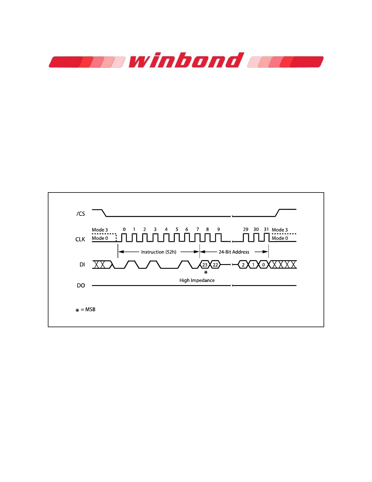
9.2.16 32KB Block Erase (52h)
The Block Erase instruction sets all memory within a specified block (32K-bytes) to the erased state of
all 1s (FFh). A Write Enable instruction must be executed before the device will accept the Block Erase
Instruction (Status Register bit WEL must equal 1). The instruction is initiated by driving the /CS pin low
and shifting the instruction code “52h” followed a 24-bit block address (A23-A0) (see Figure 2). The
Block Erase instruction sequence is shown in figure 16.
The /CS pin must be driven high after the eighth bit of the last byte has been latched. If this is not done
the Block Erase instruction will not be executed. After /CS is driven high, the self-timed Block Erase
instruction will commence for a time duration of tBE1 (See AC Characteristics). While the Block Erase
cycle is in progress, the Read Status Register instruction may still be accessed for checking the status
of the BUSY bit. The BUSY bit is a 1 during the Block Erase cycle and becomes a 0 when the cycle is
finished and the device is ready to accept other instructions again. After the Block Erase cycle has
finished the Write Enable Latch (WEL) bit in the Status Register is cleared to 0. The Block Erase
instruction will not be executed if the addressed page is protected by the Block Protect (SEC, TB, BP2,
BP1, and BP0) bits (see Status Register Memory Protection table).
Figure 16. 32KB Block Erase Instruction Sequence Diagram
- 29 -
Publication Release Date: October 14, 2009
Preliminary -- Revision A
Share Link: 