W89C92 Ver la hoja de datos (PDF) - Winbond
Número de pieza
componentes Descripción
Lista de partido
W89C92 Datasheet PDF : 11 Pages
| |||
W89C92
PCB Layout Guidelines
(1) VDD and VSS should be connected to ground and a -9V DC copper plane, respectively, to dissipate
the power heat. The overlapped power and ground copper plane form a coupling capacitor that can
decouple high frequency noise on the power line. The -9V DC and ground must be as close as
possible to VDD and VSS of the W89C92 to reduce line inductance. A good power plane layout will
improve the MTBF of the W89C92.
(2) The trace between the coaxial cable and RXI and the isolating diode should be made as short as
possible. All the metal traces and the copper plane should be as far as possible from the RXI trace. A
longer RXI trace will induce more shunt capacitance loading, while closer traces induce larger
capacitance. This extra capacitance may overload the coaxial cable beyond the 2 pF stated in the
IEEE 802.3 specification. The RXI trace should be made as thick as possible to reduce the line
inductance. The maximum length of the RXI trace, 4 cm, is recommended.
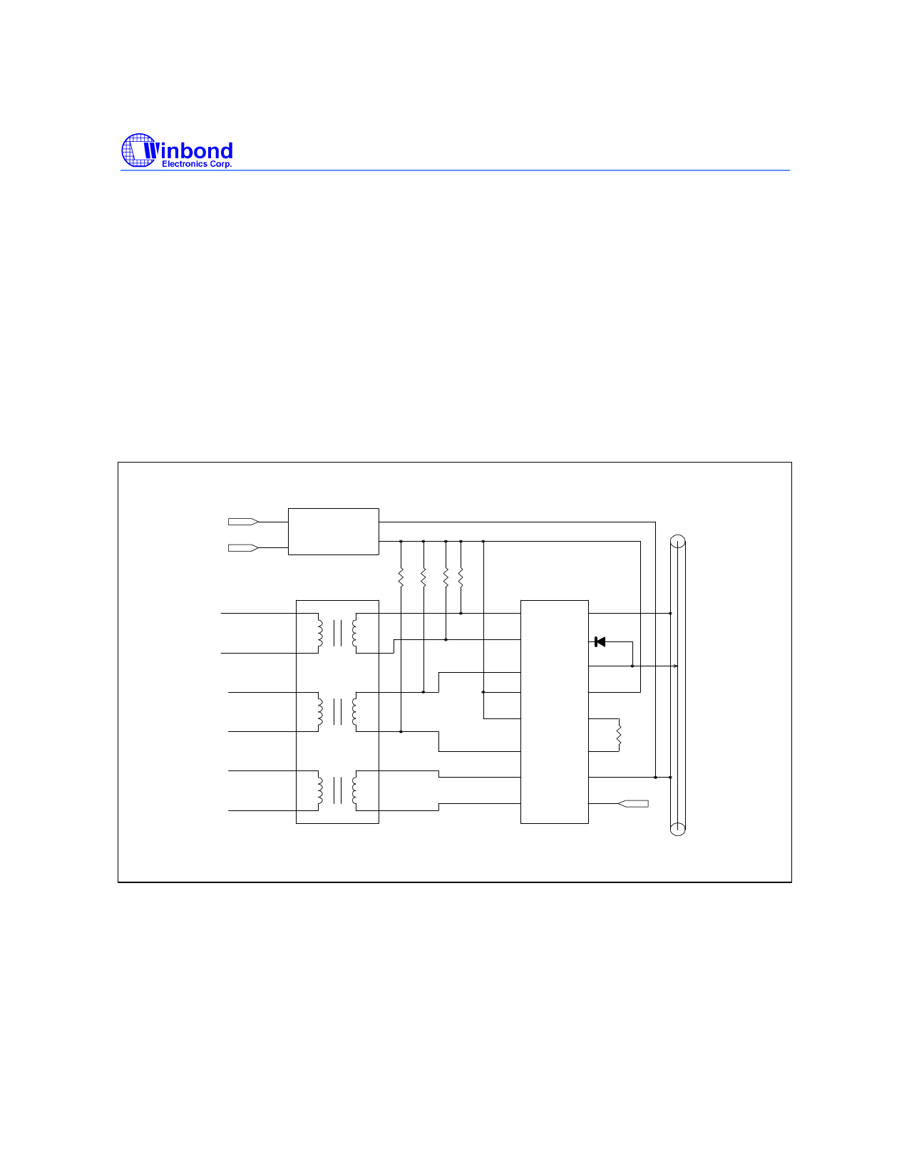
A Cheapernet MAU implementation with the TCC
+
5V
_
DC to DC
Converter
1.5K Each
9V (Isolated)
+
−
COAX
1
16
2
15
4
13
5
12
7
10
8
9
CSO+
1
CSO-
2
CLS
16
TXO
15 1N4148
DI+
3
W
8
RXI
14
VSS
9
4C
13 VSS
9
VSS
52
ER-
12
DI-
T
C
ER+ 1 k 1%
6 C 11
DO+
7
VDD
10
DO-
8
SQE
9
- 10 -
Share Link: 