MFC1000 Ver la hoja de datos (PDF) - Conexant Systems
Número de pieza
componentes Descripción
Lista de partido
MFC1000 Datasheet PDF : 16 Pages
| |||
Hardware Description
The MFC1000 hardware interface signals are shown
in Figure 2.
Note: Suffix n indicates an active low signal.)
MFC1000 Controller
The MFC1000 Controller contains an internal RISC
Processor with a 64-Mbyte address space and
dedicated circuitry optimized for facsimile image
processing, Multifunctional peripheral control and
monitoring, and plain paper printer support.
The RISC Processor is an ARM7TDMI central
processing unit (CPU). This CPU provides fast
instruction (up to 40 MHz clock speed) execution
and memory efficient input/output bit manipulation.
The CPU connects to other internal and external
MFC1000 functions over a 16-bit data and 26-bit
address bus and dedicated control lines. A 1024-
byte instruction cache with 16-byte cache line
structure is supported. The cache memory can be
enabled or disabled by firmware.
26-bit address bus, 16-bit data bus, control, status,
interrupt, and decoded chip select signals support
connection to external ROM, external RAM, DRAM,
and optional peripheral devices. 32-bit, 16-bit, and 8-
bit CPU accesses are supported through the 16-bit
data bus.
DRAM Controller
The MFC1000 includes a DRAM controller with
single and page mode access support and EDO
DRAM support. It supports fast, normal, or slow
refresh time and battery back up. The refresh is
performed automatically and supported during
battery backup. Only CAS-before-RAS refresh is
supported. Two DRAM banks of 512K, 1MB, 4MB,
or 16MB each are supported with two CAS signals.
4, 8 and 16 bit organizations are supported; access
speeds from 50 to 80 ns are supported. The
interleave access modes are supported for DRAM
accesses.
MD192
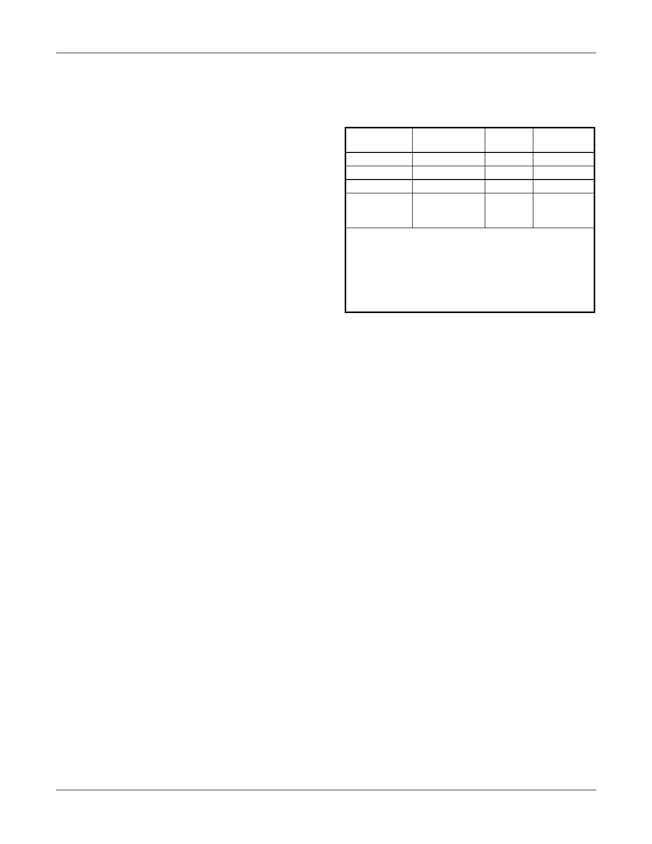
Flash Memory Controller
The MFC1000 includes a Flash Memory Controller
that supports the following types of Flash memory
and their equivalents:
Manufacturer Model Number
Size
(Kbytes)
Type
AMD
AM29F040
512
NOR
Intel
28F400BL
512
NOR
Samsung
KM29N040
512
NAND
Toshiba
TC58A040F
512
serial NAND
(using serial
interface)
Note:
1. NOR-type flash memory accesses are accomplished by
using normal bus operations.
2. NAND-type flash memory accesses are accomplished by
multiple accesses to IO address space.
3. The max. flash memory size supported by this controller
is 2M bytes.
Interrupts
Up to four external level sensitive interrupts are
provided. One active high and one active low
interrupt are provided for general use, and dedicated
active low interrupts are provided for the modem and
an external printer interface.
DMA Channels
Nine internal DMA channels support scanner,
T.4/T.6, Parallel I/O, and Data formatting (resolution
conversion and bit rotation) access of memory. One
external DMA channel supports data transfer to an
external peripheral device such as a print engine
controller. One DMA channel can be programmed as
an internal or external DMA channel and supports
either the internal scan IF or an external peripheral
device such as a image processing chip.
External RAM and ROM
External RAM/Flash memory up to 44 MB and ROM
up to 4 MB (or up to 8 MB of ROM and 40 MB of
RAM/Flash memory) can be connected to the
MFC1000 as well as external peripherals. ROM
stores all the MFC1000 ENGINE program object
code. RAM is used by the MFC1000 ENGINE
Embedded CPU as a shading RAM, image line
buffer RAM and to store some special program
object code.
Chip Selects
Various chip selects (CS) are provided by the
MFC1000 such as ROMCSn, CS0n for SRAM, CS1n
for external peripherals, MCSn for modem, and
optional general purpose chip selects CS[5:2]. The
interleave access mode is supported for the ROM
access.
Scanner Stepper Motor Control
Scanner motor stepping can be programmed to
synchronize to the scan cycle.
5
Share Link: 