XC6224 Ver la hoja de datos (PDF) - TOREX SEMICONDUCTOR
Número de pieza
componentes Descripción
Lista de partido
XC6224 Datasheet PDF : 26 Pages
| |||
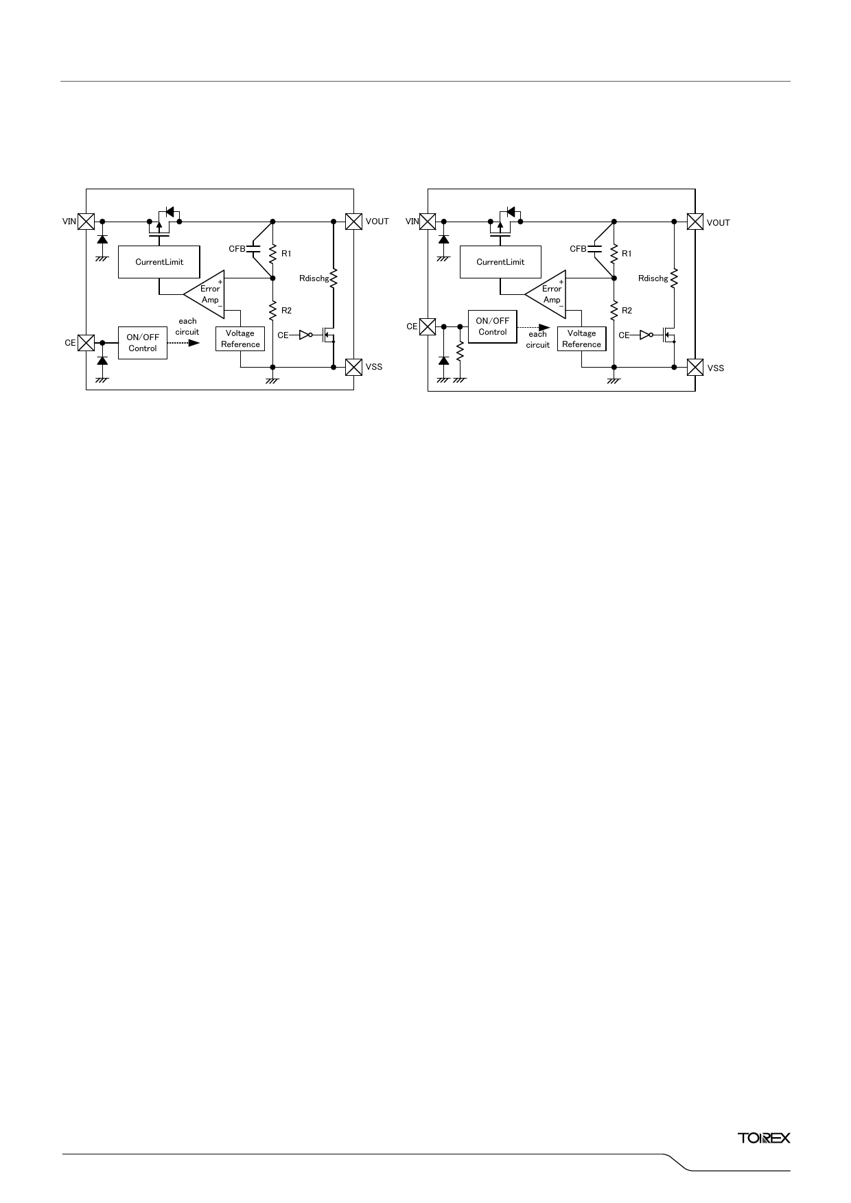
■ OPERATIONAL EXPLANATION
(1) XC6224Axxxxx
(2) XC6224Bxxxxx
XC6224
Series
The voltage divided by resistors R1 & R2 is compared with the internal reference voltage by the error amplifier. The
P-channel MOSFET which is connected to the VOUT pin is then driven by the subsequent output signal. The output voltage
at the VOUT pin is controlled and stabilized by a system of negative feedback. The current limit circuit and short circuit
protection operate in relation to the level of output current. Further, the IC’s internal circuitry can be shutdown via the CE
pin signal.
<Low ESR Capacitor>
The XC6224 needs an output capacitor CL and a built-in phase compensation circuit for phase compensation. In order
to ensure the stable phase compensation, please place an output capacitor CL of 0.47μF or bigger at the VOUT pin as close
as possible. For a stable power input, please connect an input capacitor CIN of 0.47μF between the VIN pin and the VSS
pin.
<Current Limiter, Short-Circuit Protection>
The protection circuit operates as a combination of an output current limiter and fold-back short circuit protection.
When load current reaches the current limit level, the output voltage drops. As a result, the load current starts to reduce
with showing fold-back curve. The output current finally falls at the level of 35mA when the output pin is short-circuited.
<CE Pin>
The IC's internal circuitry can be shutdown via the signal from the CE pin. In shutdown mode, output at the VOUT pin will
be pulled down to the VSS level in the XC6224B series. When the CE pin is open, the output voltage becomes undefined
state in the XC6224A series because of a high active and no pull-down. Although the CE pin is equal to CMOS input
configuration, the CE pin input current which flows into a pull-down resistor will increase in the XC6224B series
■ NOTES ON USE
1. For temporary, transitional voltage drop or voltage rising phenomenon, the IC is liable to malfunction should the ratings
be exceeded.
2. Torex places an importance on improving our products and its reliability.
However, by any possibility, we would request user fail-safe design and post-aging treatment on system or equipment.
3. Where wiring impedance is high, operations may become unstable due to the noise and/or phase lag depending on
output current. Please strengthen VIN and VSS wiring in particular.
4. The input capacitor CIN and the output capacitor CL should be placed to the IC as close as possible with a shorter wiring.
7/26
Share Link: 