UPC3211GR Ver la hoja de datos (PDF) - NEC => Renesas Technology
Número de pieza
componentes Descripción
Lista de partido
UPC3211GR Datasheet PDF : 16 Pages
| |||
PIN FUNCTIONS
Pin
Pin
No.
Name
Pin
Voltage
TYP. (V)
1
BY2
–
2
VAGC
3
GND2A
4
GND2B
5
Vcc1
0 to 3
0.0
0.0
9.0
6
Vcc2
9.0
7
GND2C
0.0
8
GND2D
0.0
9
GND2E
0.0
10
BY3
1.64
11
OUT2
6.9
12
OUT1
6.9
Function and Explanation
Non Connection pin.
This pin should be opened.
Automatic gain control pin.
Ground pins of differential amplifier.
Power supply pin of AGC amplifier
block.
Power supply pin of differential
amplifier and output block.
Ground pins of differential amplifier.
Bypass pin of regulator block.
Signal output pins.
This pins feature low-impedance
because of its emitter-follower output
port.
The pin that is not used should be
grounded through 50 ohm resistor.
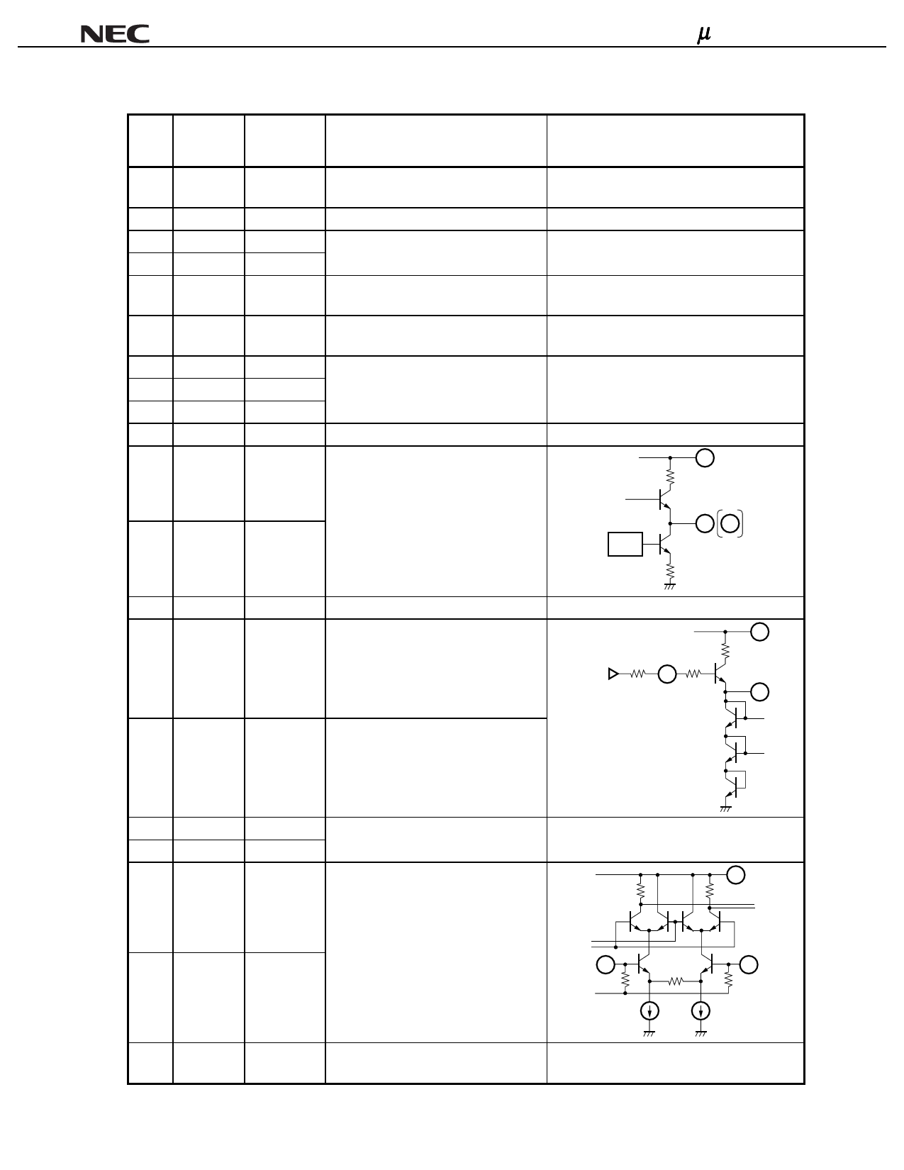
µPC3211GR
Equivalent Circuit
REG
6
11 12
13
GND3
14 PA_BIAS
0.0
2.45
Ground pin of output block.
This is the pin to feed base bias in
case of connection to transistor as
power amplifier.
15
Psave
16
GND1B
18
GND1A
17 AGC IN2
19 AGC IN1
9.0
(+5 kΩ)
0.0
0.0
2.43
Power-save pin.
Vcc : ON
GND : SLEEP
The 5 kΩ resistor should be
connected between 15 pin and Vcc.
Ground pin of AGC amplifier block.
Signal input pin.
In the case of single input, 17 or 19
pin should be grounded through
capacitor.
2.43
VCC
(9 V)
15
5 kΩ
19
5
14
5
17
20
BY1
–
Non Connection pin.
This pin should be opened.
Data Sheet P13564EJ3V0DS00
3
Share Link: 