RF2484 Ver la hoja de datos (PDF) - RF Micro Devices
Número de pieza
componentes Descripción
Lista de partido
RF2484 Datasheet PDF : 10 Pages
| |||
RF2484
Preliminary
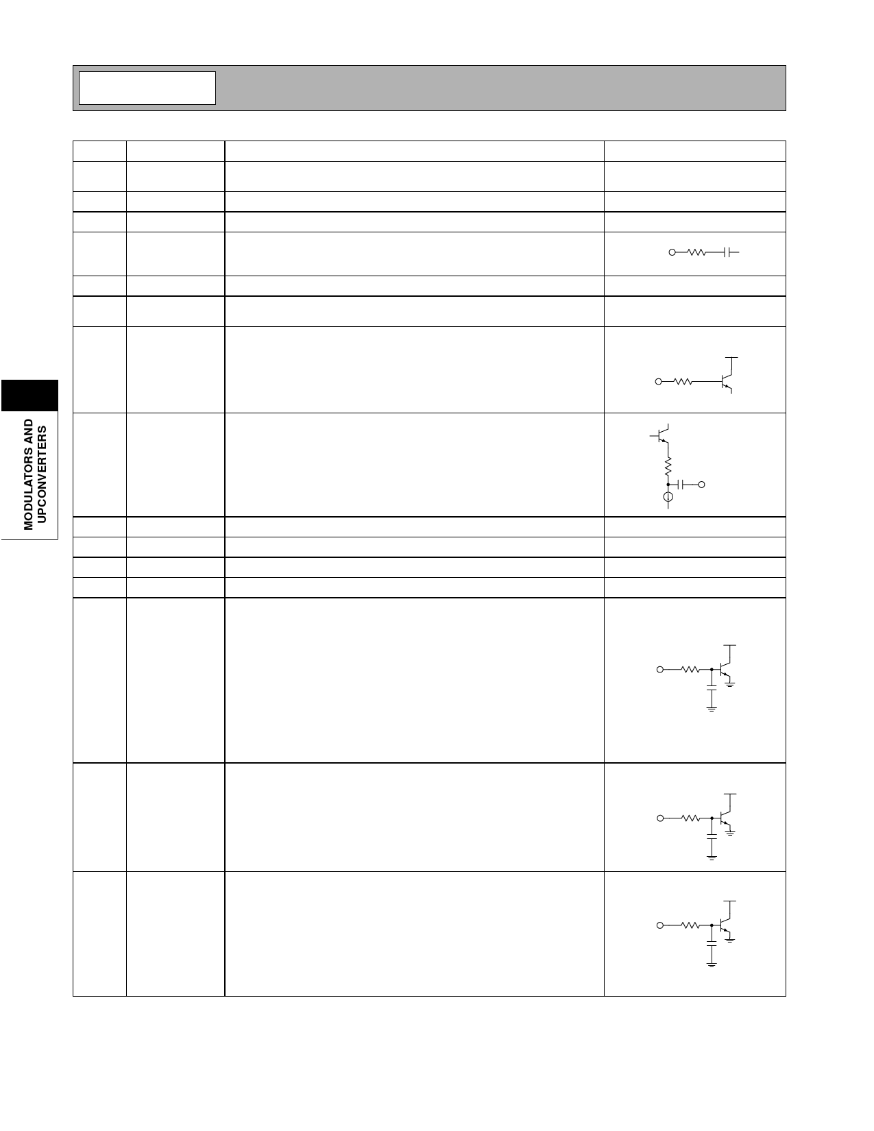
Pin Function Description
Interface Schematic
1
GND
Ground connection. This pin should be connected directly to the
ground plane.
2
GND
Same as pin 1.
3
GND
Same as pin 1.
4
LO
The input of the phase shifting network. This pin has an internal DC
blocking capacitor. This port is voltage-driven so matching at different
LO
frequencies is generally not required.
5
GND
Same as pin 1.
6
VCC
Power supply. An external capacitor is needed if no other low frequency
bypass capacitor is nearby.
7
5
PD
Power Down control. When this pin is "low," all circuits are shut off. A
"low" is typically 1.2V or less at room temperature.When this pin is
"high" (VCC), all circuits are operating normally. If PD is below VCC, out-
put power and performance will be degraded. Operating in this region
is not recommended, although it might be useful in some applications
VCC
200 Ω
PD
where power control is required.
8
RF OUT RF Output. This pin has an internal DC blocking capacitor. At some fre-
quencies, external matching may be needed to optimize output power.
A small amount of DC current may be present at this output. As a
result, if the voltage at this pin is measured using a high impedance
probe, some DC voltage may be observed at this output.
RF OUT
9
GND
Same as pin 1.
10
VCC
Same as pin 6.
11
GND
Same as pin 1.
12
GND
Same as pin 1.
13
Q SIG
Baseband input to the Q mixer. This pin is DC coupled. The input drive
level determines output power and linearity performance; for better car-
rier suppression, sideband suppression, and dynamic range, the drive
level should be as high as possible to meet the required linearity perfor-
mance. The recommended DC level for this pin is 4.1V.
For optimum carrier suppression, the DC voltages on I REF, Q REF, I
SIG and Q SIG should be adjusted slightly to compensate for inherent
undesired internal DC offsets; for optimum sideband suppression,
phase and signal amplitude on IREF, Q REF, I SIG and Q SIG should
be adjusted slightly to compensate for inherent undesired internal off-
sets. See RFMD AN0001 for more detail.
14
I SIG
Baseband input to the I mixer. This pin is DC coupled. The input drive
level determines output power and linearity performance; for better car-
rier suppression, sideband suppression, and dynamic range, the drive
level should be as high as possible to meet the required linearity perfor-
mance. The recommended DC level for this pin is 4.1V; see pin 13 for
more information.
VCC
100 Ω
1p
VCC
100 Ω
1p
15
I REF
Reference voltage for the I mixer. This voltage should be the same as
the DC voltage supplied to the I SIG pin. A voltage of 4.1V is recom-
mended; see pin 13 for more information.
The SIG and REF inputs are inputs of a differential amplifier. Therefore
the REF and SIG inputs are interchangeable. If swapping the I SIG and
I REF pins, the Q SIG and Q REF also need to be swapped to maintain
the correct phase. It is also possible to drive the SIG and REF inputs in
a differential mode. This will increase the gain.
VCC
100 Ω
1p
5-32
Rev A2 010829
Share Link: 