RF210A Ver la hoja de datos (PDF) - Conexant Systems
Número de pieza
componentes Descripción
Lista de partido
RF210A Datasheet PDF : 8 Pages
| |||
RF210(A/B)
Technical Description
The RF210(A/B) dual-band, image-reject downconverters
implement the front-end functions of a dual-band super-
heterodyne receiver. These devices consist of two receive
paths, one for GSM900 and the other for DCS1800 (or
PCS1900). Each receive path contains an LNA and an image-
reject mixer. The IF and LO ports are common to both receive
paths. The image-reject mixers can provide 30 dB of image
rejection for both the GSM900 and the DCS1800 (or PCS1900)
bands without using any post-LNA image reject filters.
The LNA/mixer combination has a switchable gain. The RF210A
and RF210B both have 22 dB of gain in the high gain mode. For
the RF210A, the gain is reduced by 10 dB (GSM band) and by
8 dB (DCS/PCS band) in the low gain mode. For the RF210B,
the gain is reduced by 20 dB (GSM band) and by 16 dB
(DCS/PCS band) in the low gain mode. The gain mode is
selected using the GAINSEL pin (Pin 7). Low gain mode is
selected by driving the GAINSEL signal high; high gain mode is
selected by driving the signal low. In addition, small adjustments
Image-Reject Downconverter
of the mixer gain can be accomplished by varying the quiescent
current on the ADJMIX pin (Pin 11). This pin can be connected
to VCC or ground through resistors. The current will increase if
the pin is connected to GND and decrease if connected to VCC.
For optimal performance, this pin should be left unconnected.
The band of operation for RF210(A/B) is selected by the
BANDSEL signal on Pin 14. It switches the receive path
between GSM900 and DCS1800 (or PCS1900) bands.
The device can operate from a three-cell battery pack (2.7 V to
5.0 V). Standby mode current is extremely low at 20 µA, which
maximizes handset standby time.
The signal pin assignments and functional pin descriptions are
found in Table 1. The absolute maximum ratings of the
RF210(A/B) are provided in Table 2, the operating conditions
are specified in Table 3, and electrical specifications are
provided in Table 4. Figure 3 shows the diagram for a typical
application circuit using the RF210(A/B) downconverter. Figure
4 provides the package dimensions for the 20-pin TSSOP
device and Figure 5 provides the tape and reel dimensions.
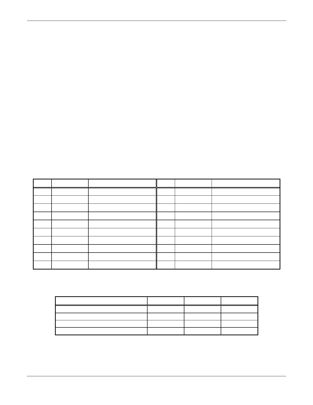
Pin #
1
2
3
4
5
6
7
8
9
10
Name
NC
LNA900GND
BIASGND
LNA900IN
BIASVCC
LNAVCC
GAINSEL
LNA1800IN
LNA1800GND
ENA
Table 1. RF210(A/B) Signal Description
Description
No connect
900 MHz LNA ground
Bias ground
900 MHz LNA input
Bias supply
LNA supply
LNA gain select
1800 MHz LNA input
1800 MHz LNA ground
Device enable (active high)
Pin #
11
12
13
14
15
16
17
18
19
20
Name
ADJMIX
LOGND
LOIN
BANDSEL
BYP1800
IFOUT–
IFOUT+
BYP900
MIXGND
MIXVCC
Description
Mixer bias adjust pin
LO input ground
LO input
Band selection pin
Bypass capacitor for 1800 MHz band
Mixer output (negative)
Mixer output (positive)
Bypass capacitor for 900 MHz band
Mixer ground
Mixer supply
Parameter
Storage Temperature
LNA Input Power
Supply Voltage (VCC)
Input Voltage Range
Table 2. Absolute Maximum Ratings
Minimum
–40
–0.3
–0.3
Maximum
+125
+5
+6
Vcc
Units
°C
dBm
V
V
2
October 20, 1999
Conexant
Proprietary Information and Specifications are Subject to Change
100775A
Share Link: 