NCP1216A Ver la hoja de datos (PDF) - ON Semiconductor
Número de pieza
componentes Descripción
Lista de partido
NCP1216A Datasheet PDF : 18 Pages
| |||
NCP1216, NCP1216A
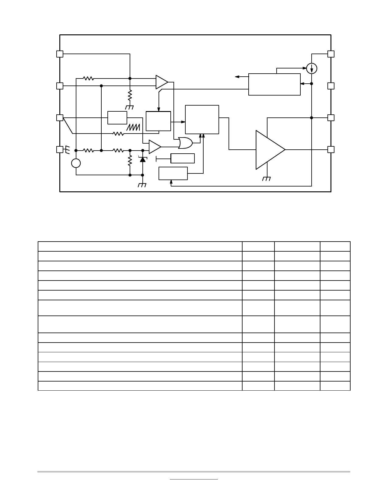
Adj 1
96 k
FB 2
1.1 V
25 k
Skip Cycle Comparator
+
Internal VCC
−
Clock Jittering
HV Current Source
UVLO High and Low
Internal Regulator
Current 3
Sense
GND 4
220 ns
L.E.B
19 k
Ramp
20 k
Compensation
Pull−up Resistor 57 k
+
−
Vref
25 k
5V
65 kHz
100 kHz
133kHz
Set Q Flip−Flop Q
DCmax = 75%
Reset
+
−
1V
1 ms SS*
Overload?
Fault Duration
* Available for ”A” version only.
Figure 2. Internal Circuit Architecture
$500 mA
8 HV
7 NC
6 VCC
5 Drv
MAXIMUM RATINGS
Rating
Symbol
Value
Unit
Power Supply Voltage, VCC Pin
Maximum Voltage on Low Power Pins (except Pin 8 and Pin 6)
VCC
16
V
−0.3 to 10
V
Maximum Voltage on Pin 8 (HV), Pin 6 (VCC) Decoupled to Ground with 10 mF
Maximum Voltage on Pin 8 (HV), Pin 6 (VCC) Grounded
Minimum Operating Voltage on Pin 8 (HV)
500
V
450
V
28
V
Maximum Current into all Pins except VCC (Pin 6) and HV (Pin 8) when 10 V ESD Di-
odes are Activated
5.0
mA
Thermal Resistance Junction−to−Air, PDIP−7 Version
Thermal Resistance Junction−to−Air, SOIC−8 Version
Maximum Junction Temperature
Temperature Shutdown
RqJ−A
100
°C/W
RqJ−A
178
TJMAX
150
°C
TSD
155
°C
Hysteresis in Shutdown
30
°C
Storage Temperature Range
−60 to +150
°C
ESD Capability, HBM Model (All Pins except VCC and HV)
2.0
kV
ESD Capability, Machine Model
200
V
Stresses exceeding those listed in the Maximum Ratings table may damage the device. If any of these limits are exceeded, device functionality
should not be assumed, damage may occur and reliability may be affected.
1. This device series contains ESD protection rated using the following tests:
Human Body Model (HBM) 2000 V per JEDEC Standard JESD22, Method A114E.
Machine Model (MM) 200 V per JEDEC Standard JESD22, Method A115A.
www.onsemi.com
3
Share Link: 