MB2646BB Ver la hoja de datos (PDF) - Philips Electronics
Número de pieza
componentes Descripción
Lista de partido
MB2646BB Datasheet PDF : 16 Pages
| |||
Philips Semiconductors Products
Dual octal bus transceiver/registers (3-State)
Product specification
MB2646
DESCRIPTION (continued)
The select (nSAB, nSBA) pins determine
whether data is stored or transferred through
the device in real-time. The nDIR determines
which bus will receive data when the nOE is
active Low. In the isolation mode (nOE =
High), data from Bus A may be stored in the
B register and/or data from Bus B may be
stored in the A register. When an output
function is disabled, the input function is still
enabled and may be used to store and
transmit data. Only one of the two buses, A
or B may be driven at a time.
PIN DESCRIPTION
PIN NUMBER
48, 45, 19, 22
49, 44, 18, 23
47, 20
50, 51, 1, 2, 3, 5, 6, 7,
8, 9, 10, 11, 12, 13, 15, 16
42, 41, 39, 38, 37, 36, 35, 34,
33, 32, 31, 29, 28, 27, 25, 24
46, 21
4, 17, 30, 43
14, 26, 40, 52
SYMBOL
1CPAB, 1CPBA, 2CPAB, 2CPBA
1SAB, 1SBA, 2SAB, 2SBA
1DIR, 2DIR
1A0 – 1A7,
2A0 – 2A7
1B0 – 1B7,
2B0 – 2B7
1OE, 2OE
GND
VCC
NAME AND FUNCTION
Clock input A to B / Clock input B to A
Select input A to B / Select input B to A
Direction control inputs
Data inputs/outputs (A side)
Data inputs/outputs (B side)
Output enable inputs
Ground (0V)
Positive supply voltage
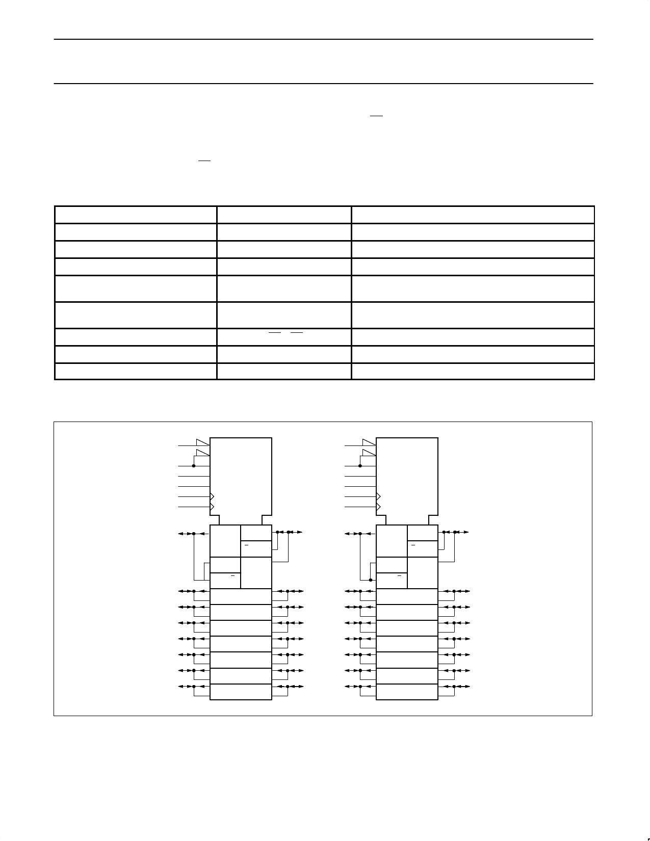
LOGIC SYMBOL (IEEE/IEC)
46
G3
3EN1 [BA]
47
3EN2 [AB]
44
G6
49
G7
45
C4
48
C5
21
G3
3EN1 [BA]
20
3EN2 [AB]
23
G6
18
G7
22
C4
19
C5
50
≥1
6 4D
∇1
42
8
≥1
6 4D
∇1
33
61
61
5D 7
17
≥1
2∇
5D 7
17
≥1
2∇
51
41
9
32
1
39
10
31
2
38
11
29
3
37
12
28
5
36
13
27
6
35
15
25
7
34
16
24
August 23, 1993
2
Share Link: 