MX641DW Ver la hoja de datos (PDF) - MX-COM Inc
Número de pieza
componentes Descripción
Lista de partido
MX641DW Datasheet PDF : 16 Pages
| |||
Dual SPM Detector
2. Signal List
4
MX641 PRELIMINARY INFORMATION
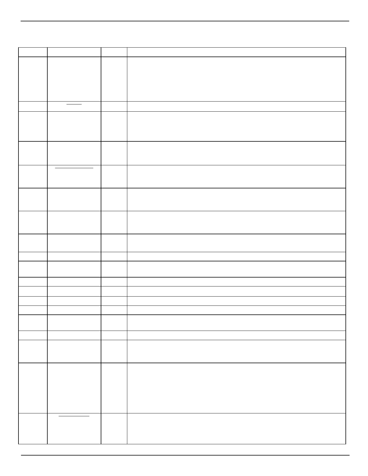
Pin No.
1
2
3
4
5
6
7
8
9
10
11
12
13
14
15
16
17
18
19
Name
Xtal/Clock
XTAL
Clock Out
Clock In
Output Enable
Ch 2 Output
Ch 1 Output
VBIAS
Ch 1 Amp Out
Ch 1 Amp In (-):
Ch 1 Amp In (+):
VSS
N/C
Ch 2 Amp In (+):
Ch 2 Amp In (-):
Ch 2 Amp Out
Output Select
Preset Level
Chip Select
Type
input
output
output
input
input
output
output
power
output
input
input
power
input
input
output
input
input
input
Description
The input to the on-chip clock oscillator; for use with a 3.579545MHz Xtal in
conjunction with the Xtal output; circuit components are on-chip. When using a
Xtal input, the Clock Out pin should be connected directly to the Clock In pin. If
a clock pulse input is used at the Clock In pin, this (Xtal/Clock) pin must be
connected directly to VDD (see Figure 2). See Figure 3 for details of clock
frequency distribution.
The output of the on-chip clock oscillator inverter.
The buffered output of the on-chip-clock oscillator inverter. If a Xtal input is
used, this output should be connected directly to the Clock In pin. This output
can support up to 3 additional MX641 ICs. See Figure 3 for details of clock
frequency distribution.
The 3.579545 clock pulse input to the internal clock dividers. If an externally
generated clock pulse input is used, the Xtal/Clock input pin should be
connected to VDD.
For multi-chip output multiplexing; controls the state of both Ch1 and Ch2
outputs. When this input is placed high (logic '1') both outputs are set to a high
impedance. When placed low (logic '0') both outputs are enabled.
The digital output of the Channel 2 SPM detector when enabled. The format of
the signal at this pin, in common with Ch 1, is selectable to either
'Tone Follower' or 'Packet' mode via the Output Select input.
The digital output of the Channel 1 SPM detector when enabled. The format of
the signal at this pin, in common with Ch 2, is selectable to either
'Tone Follower' or 'Packet' mode via the Output Select input.
The output of the on-chip analog bias circuitry. Held internally at VDD/2, this
pin should be decoupled to VSS (see Figure 2).
The output of the Channel 1 Input Amplifier. See Figure 2 and Figure 8.
The negative input to the Channel 1 Input Amplifier. See Figure 2 and Figure
8.
The positive input to the Channel 1 Input Amplifier. See Figure 2 and Figure 8.
Negative supply (GND).
No internal connection; leave open circuit.
The positive input to the Channel 2 Input Amplifier. See Figure 2 and Figure 8.
The negative input to the Channel 2 Input Amplifier. See Figure 2 and Figure
8.
The output of the Channel 2 Input Amplifier. See Figure 2 and Figure 8.
A logic input to set the Channel 1 and Channel 2 output modes. When high
(logic '1'), the outputs are in the Tone Follower mode; when low (logic '0'), the
outputs are in the Packet mode.
A logic input to set the sensitivity mode of the MX641. When high (logic '1'),
both channels are in the Fixed Sensitivity mode. The external components
govern the input sensitivity; the System Select input selects 12kHz or 16kHz
operation. When low (logic '0'), both channels are in the Controlled Sensitivity
mode. Device sensitivities and system selection are via the Chip Select/Serial
Data/Serial Clock inputs. This input has an internal pullup resistor on chip
(Fixed Sensitivity Mode).
The Chip Select input for use in data loading when using the MX641 in the
Controlled Sensitivity mode (see Figure 9). The device is selected when this
input is set low (logic '0'). When the MX641 is in the Fixed Sensitivity mode
this input should be connected to either VSS or VDD.
© 1998 MXxCOM Inc.
www.mxcom.com Tele: 800 638-5577 910 744-5050 Fax: 910 744-5054
Doc. # 20480115.003
4800 Bethania Station Road, Winston-Salem, NC 27105-1201 USA
All trademarks and service marks are held by their respective companies.
Share Link: 