TA44910W Ver la hoja de datos (PDF) - Dynex Semiconductor
Número de pieza
componentes Descripción
Lista de partido
TA44910W Datasheet PDF : 12 Pages
| |||
TA449..W
Notes:
1. dI/dt = 100A/µs.
2. VD ≤ 600V.
3. VR = 1V.
4. R.C. snubber. C = 0.22µF, R = 4.7Ω.
4. Double side cooled.
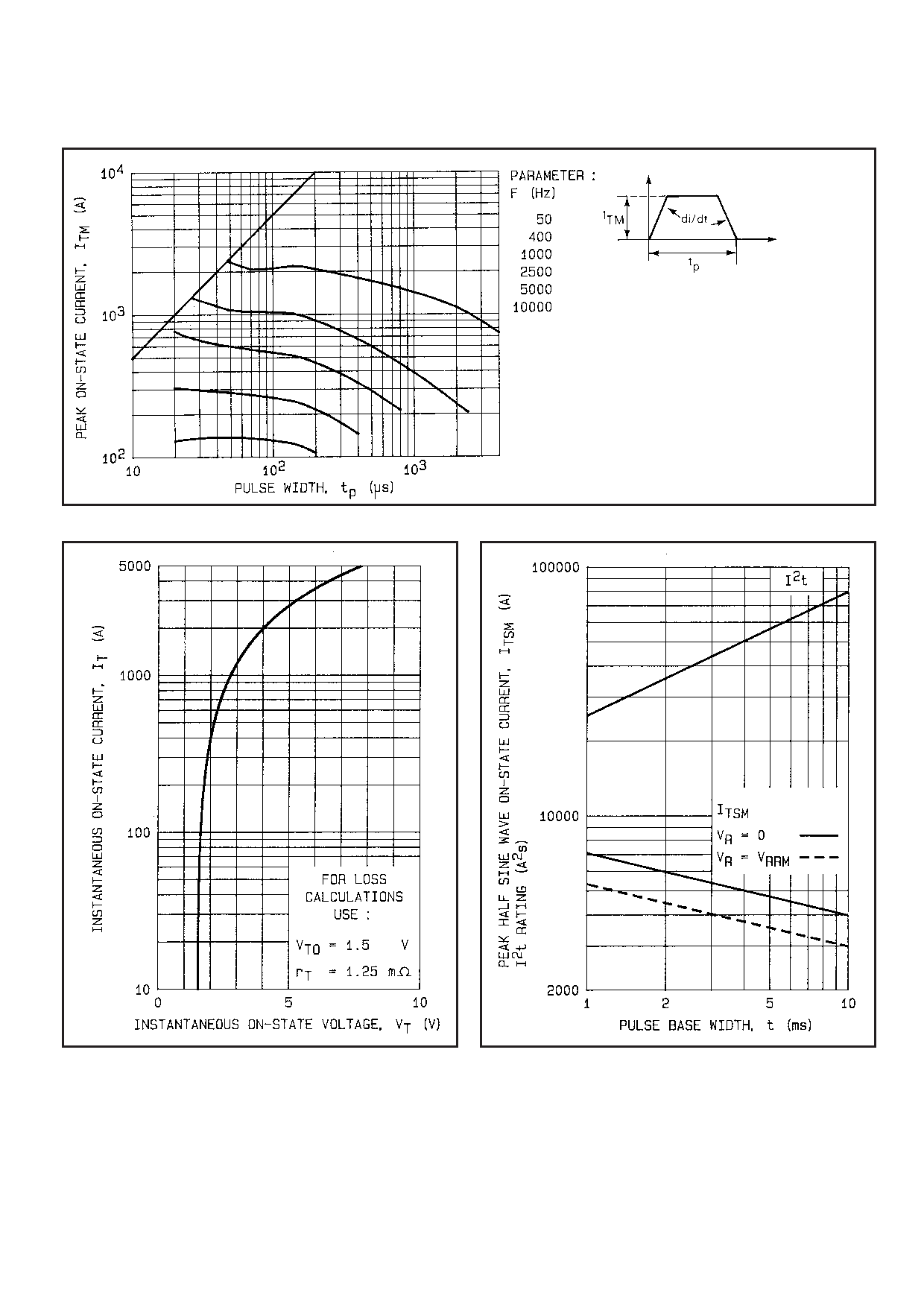
Fig.12 Maximum allowable peak on-state current vs pulse width for Tcase = 90˚C.
Fig.13 Maximum on-state conduction characteristic (Tj =
125˚C)
Fig.14 Non-repetitove sub-cycle surge on-state current and
I2t rating. (Initial Tj = 125˚C)
9/12
Share Link: 