AD74322 Ver la hoja de datos (PDF) - Analog Devices
Número de pieza
componentes Descripción
Lista de partido
AD74322 Datasheet PDF : 20 Pages
| |||
AD74322
PRELIMINARY TECHNICAL DATA
FUNCTIONAL DESCRIPTION
ADC Section
There are two ADC channels in the AD74322, configured as a stereo
pair. Each ADC channel can be independently muted. The input pins
are switched between differential inputs or four single ended inputs
accordingly. The gain block can be programmed for independent left and
right gains, in steps of +3dB, from 0dB to +12dB. The ADC operates at
an oversampling ratio of 128 and the decimation filter reduces the output
to the standard sample rates. The output maximum
sample rate is 96 kHz at ASDATA.
Automatic Level Control
Reference
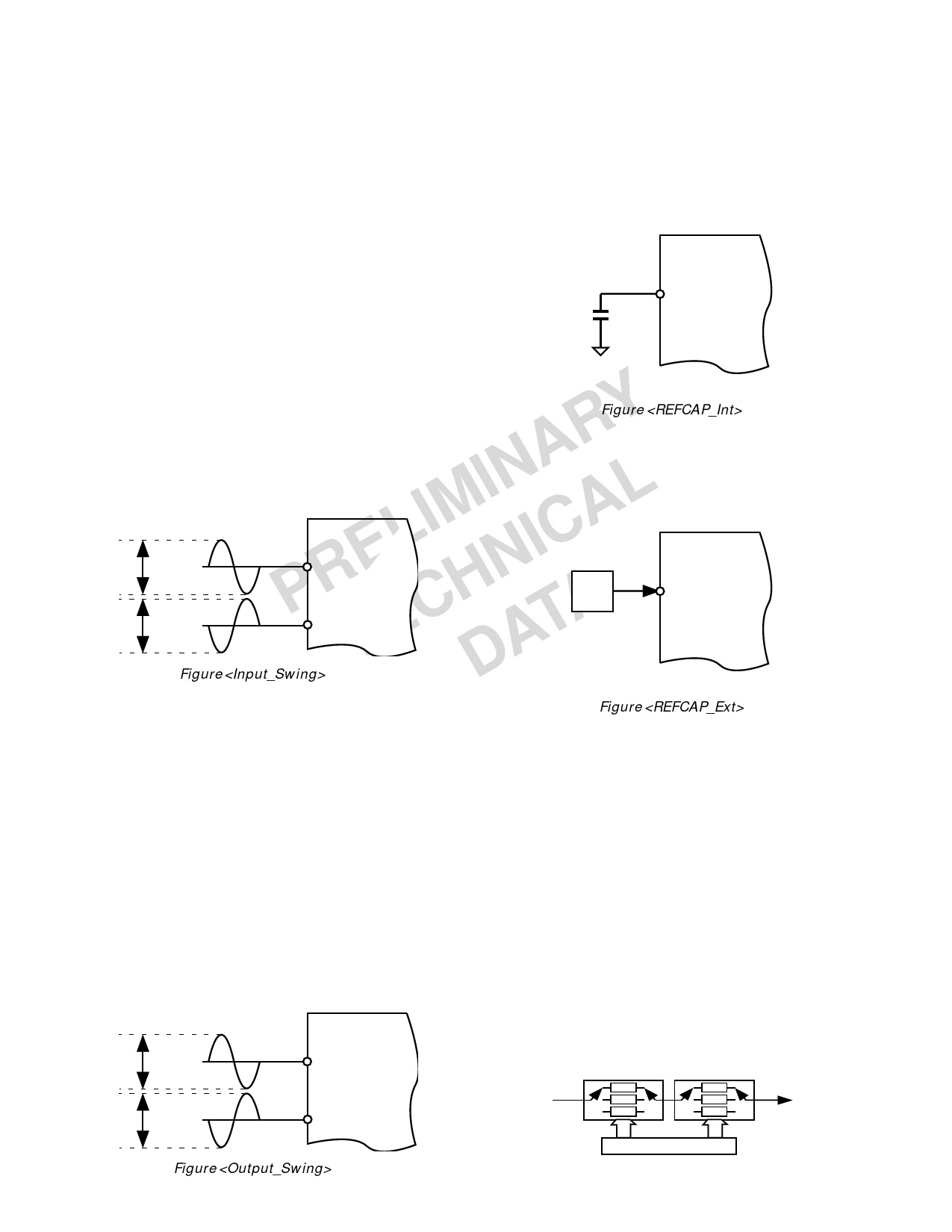
The AD74322 features an on-chip reference whose
nominal value is 1.125 V.A __ nF capacitor applied at the
REFCAP pin is necessary to stabilise the referrence. (See
Figure <REFCAP_Int>)
AD743xx
REFCAP
Analog Sigma Delta Modulator
Decimator Section
The digital decimation filter has a passband ripple of ±0.01dB and a
stopband attenuation of 70dB. The filter is an FIR type with a linear
phase response. The group delay at 48kHz is ??us. Output sample rates
up to 96 kHz are supported.
RY Input Signal swing
Each ADC input has an input range of 0.5 VRMS / 1.414 VP-P (Single-
A Ended) about a bias point equal to VREFCAP (See Figure
IN <Input_Swing>)
Figure <REFCAP_Int>
If it is required to use an external reference, because of its value or its
reference tempco, the internal reference can be disabled via Control
Register __ and the external reference applied at the REFCAP pin (See
Figure <REFCAP_Ext>).
ELIM ICAL 1.414VP-P VREFCAP
AD743xx
VINPx
PR CHN A 1.414 V P-P VREFCAP
VINNx
TE DAT Figure<Input_Swing>
1.0 V
EXTERNAL
REFERENCE
AD743xx
REFCAP
DAC Section
The AD74322 has two DAC channels arranged as a stereo pair, with two,
fully differential voltage, analog outputs for improved noise and distortion
performance. Each channel has it’s own independently programmable
attenuator with a maximum attenuation of 63dB, adjustable in 1dB steps.
Digital inputs are via a serial data input pin and a common frame
(DLRCLK) and bit (DBLCK) clock or using a ‘packed data’ mode, both
channels can be input using a single data pin.
Interpolator Section
Digital Sigma Delta Modulator
DAC
Analog Output Filter
Output Signal swing
Each ADC input has an output range of 0.5 VRMS / 1.414 VP-P (Single-
Ended) about a bias point equal to VREFCAP (See Figure
<Output_Swing>)
Figure <REFCAP_Ext>
Master Clocking Scheme
The update rate of the AD74322’s ADC and DAC channels require an
internal master clock (IMCLK) which is 256 times that sample update
rate (IMCLK = 256 * FS). In order to provide some flexibility in
selecting sample rates, the device has a series of three
master clock pre-scalers which are programmable and
allow the user to choose a range of convenient sample
rates from a single external master clock. The master
clock signal to the AD74322 is applied at the MCLK pin.
The MCLK signal is passed through a series of two
programmable MCLK pre-scalers (divider) circuits which
can be selected to reduce the resulting Internal MCLK
(IMCLK) frequency if required. The first MCLK pre-
scaler provides divider ratios of /1 (pass through), /2, /3
while the second pre-scaler provides divider ratios of ./1
(pass through), /2, /4 and the third pre-scaler provides
ratios of /1 (pass through), /2 and /5..
1.414 V P-P VREFCAP
AD743xx
VOUTPx
1.414 V P-P VREFCAP
VOUTNx
Figure <Output_Swing>
MCLK
Programmable
MCLK
Divider
Pre-Scaler 1
Pre-Scaler 2
/1
/1
/2
/2
/3
/4
IMCLK
Control Reg
–8–
Pr D 03/00
Share Link: 