AD7482 Ver la hoja de datos (PDF) - Analog Devices
Número de pieza
componentes Descripción
Lista de partido
AD7482 Datasheet PDF : 16 Pages
| |||
AD7482
Thus, the power dissipated during each cycle is:
27 mW + 42 mW = 69 mW
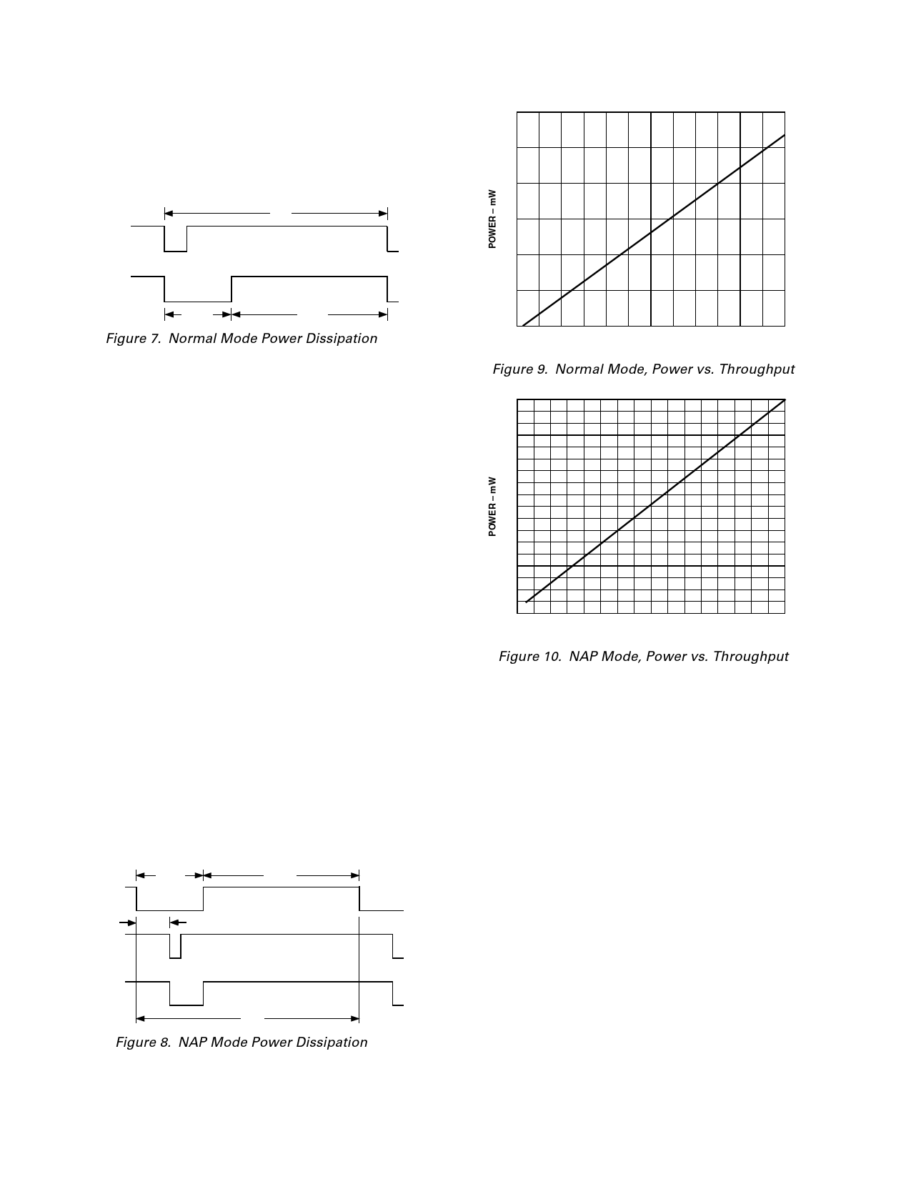
Figure 7 shows the AD7482 conversion sequence operating in
normal mode.
1 s
CONVST
BUSY
300 ns
700 ns
Figure 7. Normal Mode Power Dissipation
In NAP Mode, almost all the internal circuitry is powered down.
In this mode, the power dissipation of the AD7482 is reduced
to 2.5 mW. When exiting NAP Mode, a minimum of 300 ns
when using an external reference must be waited before initiat-
ing a conversion. This is necessary to allow the internal
circuitry to settle after power-up and for the track-and-hold to
properly acquire the analog input signal. The internal reference
cannot be used in conjunction with the NAP Mode.
If the AD7482 is put into NAP Mode after each conversion, the
average power dissipation will be reduced, but the throughput rate
will be limited by the power-up time. Using the AD7482 with a
throughput rate of 500 kSPS while placing the part in NAP
Mode after each conversion would result in average power dissi-
pation as follows:
The power-up phase contributes:
(300 ns/2 µs) × (5 V × 12 mA) = 9 mW
The conversion phase contributes:
(300 ns/2 µs) × (5 V × 18 mA) = 13.5 mA
While in NAP Mode for the rest of the cycle, the AD7482
dissipates only 1.75 mW of power.
(1400 ns/2 µs) × (5 V × 0.5 mA) = 1.75 mW
Thus, the power dissipated during each cycle is:
9 mW + 13.5 mW + 1.75 mW = 24.25 mW
Figure 8 shows the AD7482 conversion sequence if putting the
part into NAP Mode after each conversion.
NAP
CONVST
600ns
300ns
1400ns
90
85
80
75
70
65
60
0
500
1000
1500
2000
2500
3000
THROUGHPUT – kSPS
Figure 9. Normal Mode, Power vs. Throughput
90
80
70
60
50
40
30
20
10
0
0
250 500 750 1000 1250 1500 1750 2000
THROUGHPUT – kSPS
Figure 10. NAP Mode, Power vs. Throughput
In Standby Mode, all the internal circuitry is powered down and
the power consumption of the AD7482 is reduced to 10 µW. The
power-up time necessary before a conversion can be initiated is
longer because more of the internal circuitry has been powered
down. In using the internal reference of the AD7482, the ADC
must be brought out of Standby Mode 500 ms before a conver-
sion is initiated. Initiating a conversion before the required
power-up time has elapsed will result in incorrect conversion
data. If an external reference source is used and kept powered
up while the AD7482 is in Standby Mode, the power-up time
required will be reduced to 80 s.
BUSY
2 s
Figure 8. NAP Mode Power Dissipation
Figures 9 and 10 show a typical graphical representation of
power versus throughput for the AD7482 when in normal and
NAP Modes, respectively.
–10–
REV. 0
Share Link: 