ADL5390ACPZ-REEL7(RevA) Ver la hoja de datos (PDF) - Analog Devices
Número de pieza
componentes Descripción
Lista de partido
ADL5390ACPZ-REEL7 Datasheet PDF : 23 Pages
| |||
ADL5390
PIN CONFIGURATION AND FUNCTION DESCRIPTIONS
VPRF 1
QFLP 2
QFLM 3
QBBP 4
QBBM 5
VPS2 6
ADL5390
TOP VIEW
(Not to Scale)
18 VPRF
17 IFLP
16 IFLM
15 IBBP
14 IBBM
13 DSOP
Data Sheet
NOTES
1. THE EXPOSED PADDLE ON THE UNDERSIDE
OF THE PACKAGE SHOULD BE SOLDERED
TO A LOW THERMAL AND ELECTRICAL
IMPEDANCE GROUND PLANE.
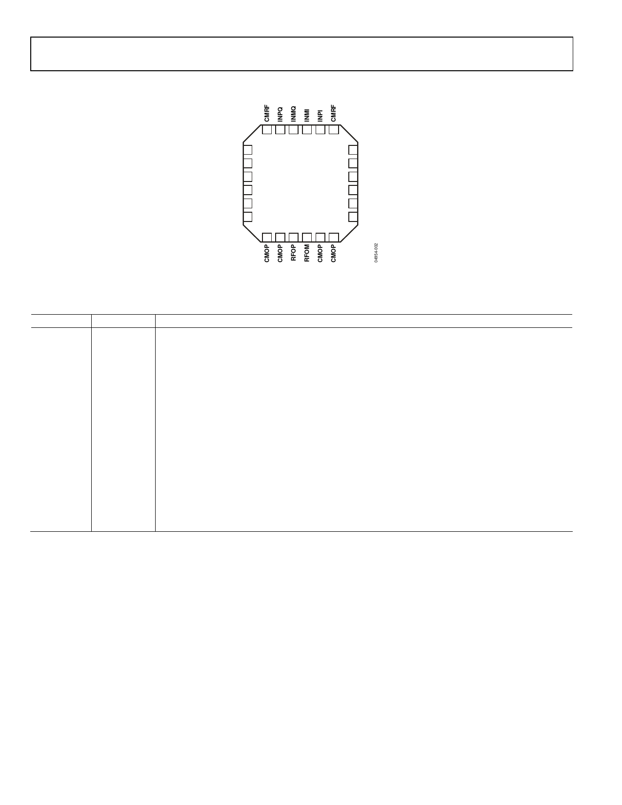
Figure 2. LFCSP Pin Configuration
Table 3. Pin Function Descriptions
Pin No.
Mnemonic Description
2, 3
QFLP, QFLM Q Baseband Input Filter Pins. Connect optional capacitor to reduce Q baseband gain control channel low-
pass corner frequency.
4, 5
QBBP, QBBM Q Channel Differential Baseband Gain Control Inputs. Typical common-mode bias level of 0.5 V.
6, 1, 18
VPS2, VPRF Positive Supply Voltage. VP of 4.75 V to 5.25 V.
7, 8, 11, 12, CMOP, CMRF Device Common. Connect via lowest possible impedance to external circuit common.
19, 24
9, 10
RFOP, RFOM Differential RF Outputs. Must be ac-coupled. Differential impedance 50 Ω nominal.
13
DSOP
Output Disable. Pull high to disable output stage. Connect to common for normal operation.
14, 15
IBBM, IBBP
I Channel Differential Baseband Gain Control Inputs. Typical common-mode bias level of 0.5 V.
16, 17
IFLM, IFLP
I Baseband Input Filter Pins. Connect optional capacitor to reduce I baseband gain control channel low-
pass corner frequency.
20, 21
INPI, INMI
I Channel Differential RF Inputs. Must be ac-coupled. 250 Ω impedance to common on each pin. These
inputs can be driven single-ended without any performance degradation.
22, 23
INMQ, INPQ
Q Channel Differential RF Inputs. Must be ac-coupled. 250 Ωimpedance to common on each pin. These
inputs can be driven single-ended without any performance degradation.
Exposed
Paddle
GND
The exposed paddle on the underside of the package should be soldered to a low thermal and electrical
impedance ground plane.
Rev. A | Page 6 of 23
Share Link: 